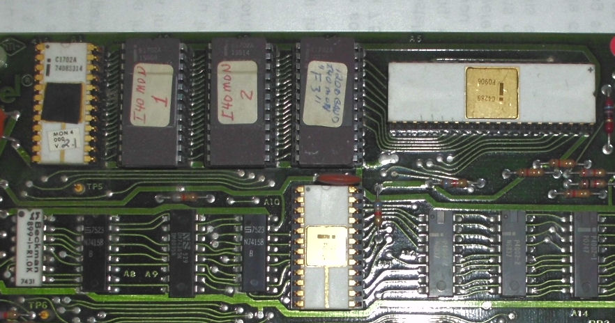
SIM-04 ROM based assembler and disassembly; SKIP instruction
To describe the next item - an Intel ROM-base native 4004 assembler for the SIM-04 4004 development board - I have to go on at length with details. That's in order to reference all the work done by other people, give them credit, leave a trail. After I did that editing, I decided to move it to its own Web page.
Here's the details of recovering the Intel/Pittman SIM-04 ROM-based assembler work done by Dwight Elvey and others. Dwight uncovered a use by Pittman of the
JCN jump-never operation Dwight/Pittman? calls "SKIP". - Herb, Nov 17 2024
Intellec 4/40 software and support from Intel
In Feb 2023 I received some 4004 4040 intellec software documents from Sid Jones, a 4/40 owner. This
sample of cover letters reveals and confirms that Intel distributed a two-pass paper tape assembler and a paper tape editor
for the 4040 system. Details forthcoming as I recieve further documents. - Herb
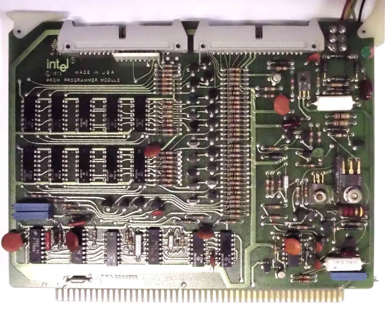
Intel Universal PROM Programmer (UPP)
Details of my Intel UPP's are now on this linked Web page.
According to the Intel Data Catalog for 1977, the Universal PROM Programmer is an Intellec system peripheral capable
of programming and verifying a number of Intel PROMS, the Intel 8748 Microcomputer (processor chip) and the Intel 8755 PROM and
I/O chip. It can hold two "personality cards" to program chips in the two PROM sockets on the front panel. The UPP-101 model has a 16 pin and 24-pin pair of PROM sockets; the UPP-102 has two 24-pin PROM sockets on the front panel. The Intel document describing the hardware is the "Intel Universal PROM Programmer Reference Manual" #9800122 or #9800133; I read the 9800133 version.
Data and control for the UPP, is performed over a 25-line "interconnection cable". The cable runs from the control board in the UPP, to an Intel Development System, running either ISIS-II or a paper-tape based Intellec System Monitor to run the "Universal PROM Mapper" program.
My cursory read of both the UPP Reference Manual and the 4/MOD-40 manual, tells me that boards between the two systems are incompatible, even though they both use a 100-pin connector and similar board dimensions.
my Intel UPP #1 and #2
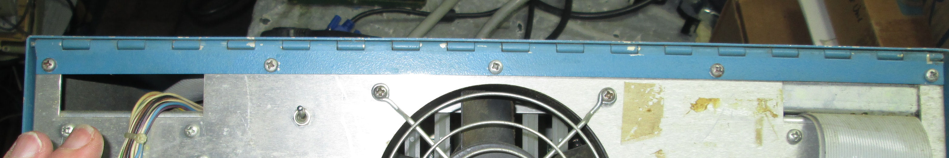
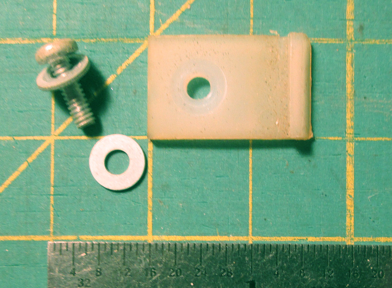
![[Intel MSC UPP]](intel440_upp_1.jpg) Here's a complete UPP or Universal PROM Programmer. It uses a 4040 processor, and was designed to be used with a terminal or with the intellec systems. There's apparently a control card and two "personality modules" for different PROM families.
Here's a complete UPP or Universal PROM Programmer. It uses a 4040 processor, and was designed to be used with a terminal or with the intellec systems. There's apparently a control card and two "personality modules" for different PROM families.
Details of my Intel UPP's are on this linked Web page.
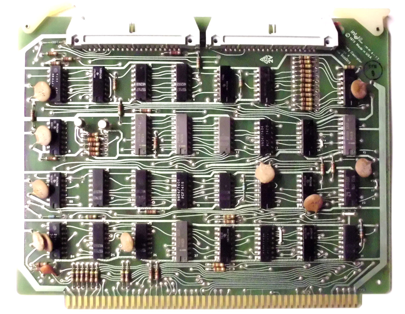
Intel intellec 8, 8/80 systems; comparison to 4-bit intellec
the Intel Intellec 8 and Intellec 8/80 chassis, looks like the MCS 4 and 4/40 chassis. Of course they use different processors. From some inspection, these have a limited "bus" structure (see the pinouts for my MCS-4/40 cards). It's not likely most cards for the 4-bit system won't work with the 8-bit system; there may be exceptions. I don't have a complete 8-bit Intellec; it's useful to list what I have on this Web page in the meantime.
intellec 4/40 vs 8/80: kinda close
In March 2023, I've changed my opinion about the relationship between the Intellec 4/40 bus and the Intellec 8/80 bus. They are both busses, and they are similar to each other. There's some possibility of cards for one, running
in the other. BUT check every board signal and check the bus-slot signals *carefully*. Slots on either system are
dedicated in various ways to specific signals and of course, DC voltages.
In Jan 2013, my colleage Kyle Owen, who owned in 2013 both an intellec 4/40 and 8/80, gave me his opinions. this is a photo of Kyle's CPU board with ROMs. In Jan 2013, Kyle looked over his Intel docs and his systems and said: "I have gone through both systems and can confirm that there would be no compatibility between an 8/80 and 4/40. Yes, they use the same 100-pin card and dimensions, but no, the bus structure is completely different. The 4/40 opted for "universal" sockets with exceptions for several of the "stock" cards like CPU, memory controller, etc., whereas the 8/80 opted for duplicate single-purpose slots. I have the [Intel] information for this." He agrees that neither systems are Multibus, a visual inspection makes that obvious. He describes the motherboards as "passive cross-wired connecting assemblies".
Intel describes their 4-bit and 8-bit Intellec systems and boards, in their 1975 "Intel Data Catalog". Thanks to that reference and discussion from Craig Andrews in Dec 2021, I took time to transcribe the board-level descriptions from that manual. In 2021 I found a copy
on the deramp.com Web site in their component/Intel/memory components archive. HOwever, apparently
I did not study these hard enough.
By early 2023, Craig Andrews developed his versions of an intellec 8008 board [details scattered on his Web site,
also see these 8008 notes]. He developed a number of replica intellec boards. In his accounts,
he suggests some compatibity between intellec RAM and ROM cards for either system which have the Intel "imm6" class name, as opposed to imm8 for 8 bit and imm4 for 4 bit. So: I compared the intellec 8/80 RAM slot signals, with the intellec 4/40 RAM slot signals. Here's a document that lists each of the bus RAM-slot signals side by side.
What those documents suggest, is that many critical intellec signals, like address and data and some signaling, are the
same for an Intel intellec RAM card for either the 4-bit 4/40 system or the 8-bit 8/80 systems. And an examination
of the backplanes for the 8/80 system, show higher-order addresses are preset per RAM or ROM slot (4 of each are on the
8-bit backplane). There's other differences, notibly DC voltages, and other signals from various other parts of the bus.
I suggest, confusion on this matter of "bus structure", is a post-1980 bias for widespread use of "universal busses",
where every slot is wired identically to every other slot. From that view, the per-slot differences on the intellec
systems, bias a conclusion based on that non-uniformity. But in the 1970's and earlier era, many computers and digital
controllers had a variety of backplanes with degrees of uniformity, or none.
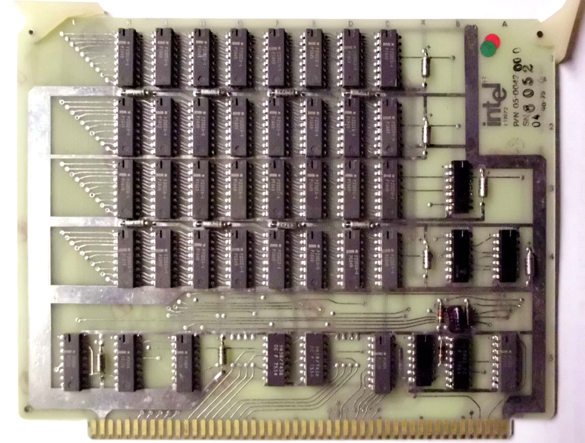
Intel intellec protoboard
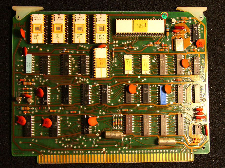
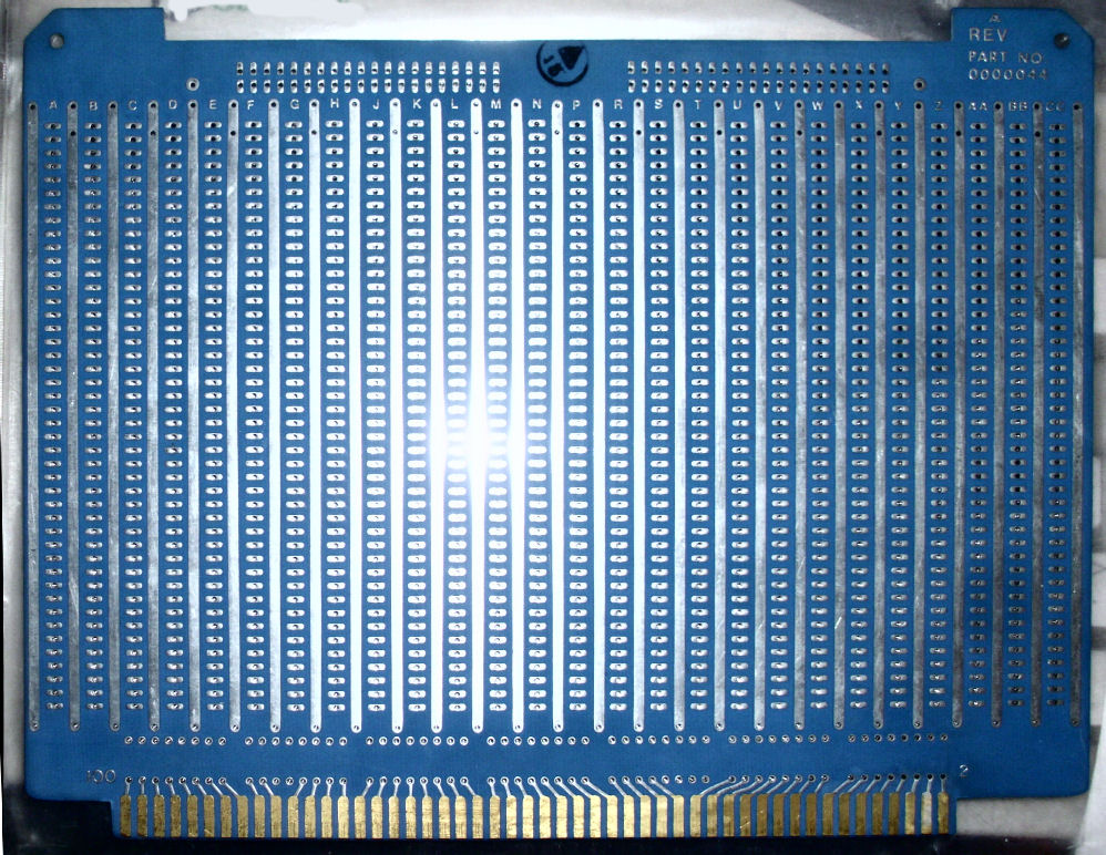
![[Intel protoboard]](intel440_proto_2.jpg) Here's an Intel protoboard for the
Intellec bus chassis. I obtained this in Nov 2013. Here's the back of the board. It's a 100-pin card but not like a S-100 bus card. The Intellec "bus" (not really a parallel bus but a collection of sometimes common lines) uses the same S-100 bus 50-pin by two edge connector (.125 inch spaced pins). None of the "bus" pins are predefined on this board. Th intel board is 8 inches wide, not ten like S-100. The Intel board is almost 6 inches tall, not 5-1/2" like the S-100. But one could cut down a generic S-100 protoboard for use.
Here's an Intel protoboard for the
Intellec bus chassis. I obtained this in Nov 2013. Here's the back of the board. It's a 100-pin card but not like a S-100 bus card. The Intellec "bus" (not really a parallel bus but a collection of sometimes common lines) uses the same S-100 bus 50-pin by two edge connector (.125 inch spaced pins). None of the "bus" pins are predefined on this board. Th intel board is 8 inches wide, not ten like S-100. The Intel board is almost 6 inches tall, not 5-1/2" like the S-100. But one could cut down a generic S-100 protoboard for use.
Intel intellec 8080 ROM monitor
Here's some results of dumping and disassembling some PROMS with early Intel 8080 monitor code.
intellec 8080 CPU
![[intellec 8080]](imm_8080.jpg) Here's an Intel intellec 8080 CPU board imm8-83. This was used in Intel's intellec 8 as an upgrade and native in the intellec 80 or 8/80. WHile
the card is the same form factor (size, edge connector) as Intel's 4004 and 4040 intellec computers, it's a very different
signal set on the bus. And the intellec 8 bus is pretty uniform, whereas the intellec 4 bus was a mix of general and dedicated signal per connector.
Here's an Intel intellec 8080 CPU board imm8-83. This was used in Intel's intellec 8 as an upgrade and native in the intellec 80 or 8/80. WHile
the card is the same form factor (size, edge connector) as Intel's 4004 and 4040 intellec computers, it's a very different
signal set on the bus. And the intellec 8 bus is pretty uniform, whereas the intellec 4 bus was a mix of general and dedicated signal per connector.
I don't have these 8-bit Intel systems so I have not yet described their architecture. - Herb
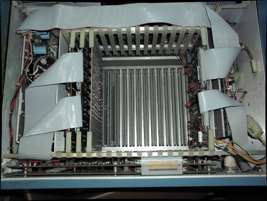
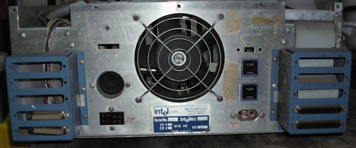
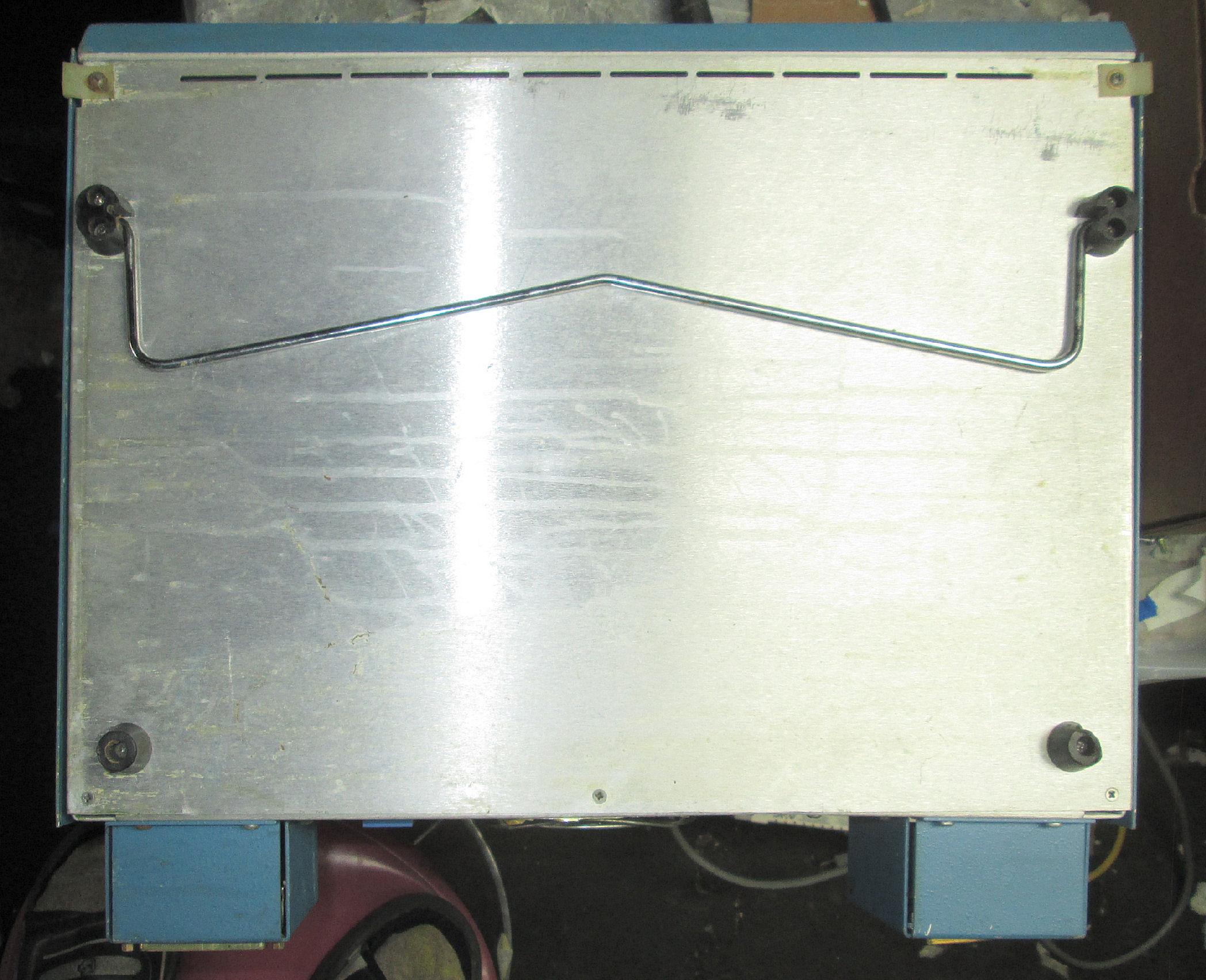
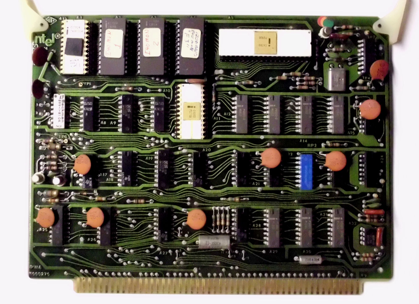
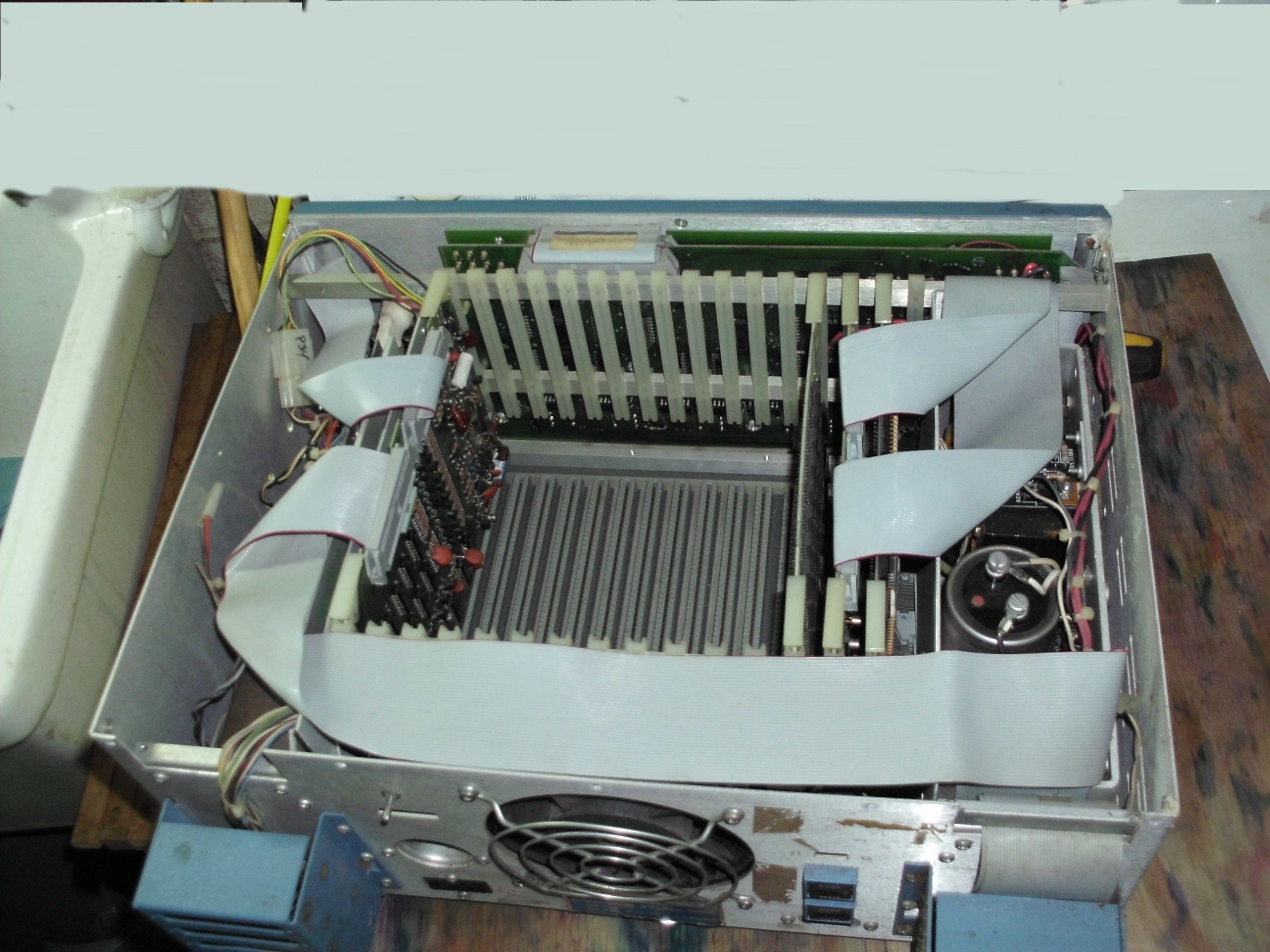
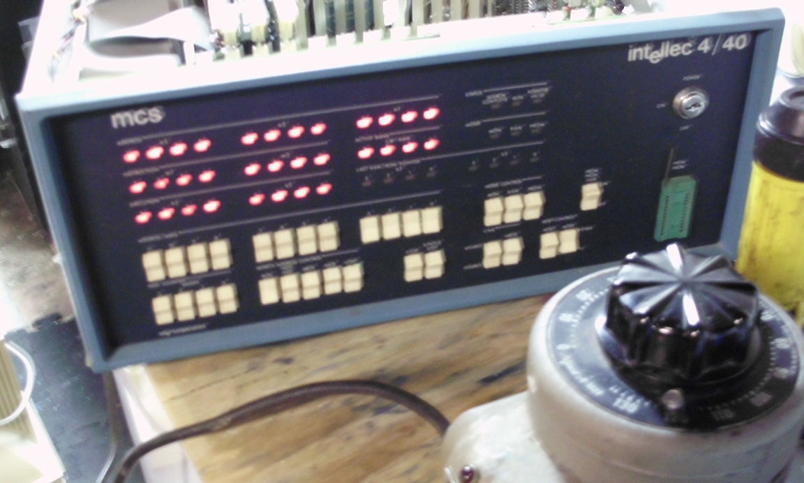
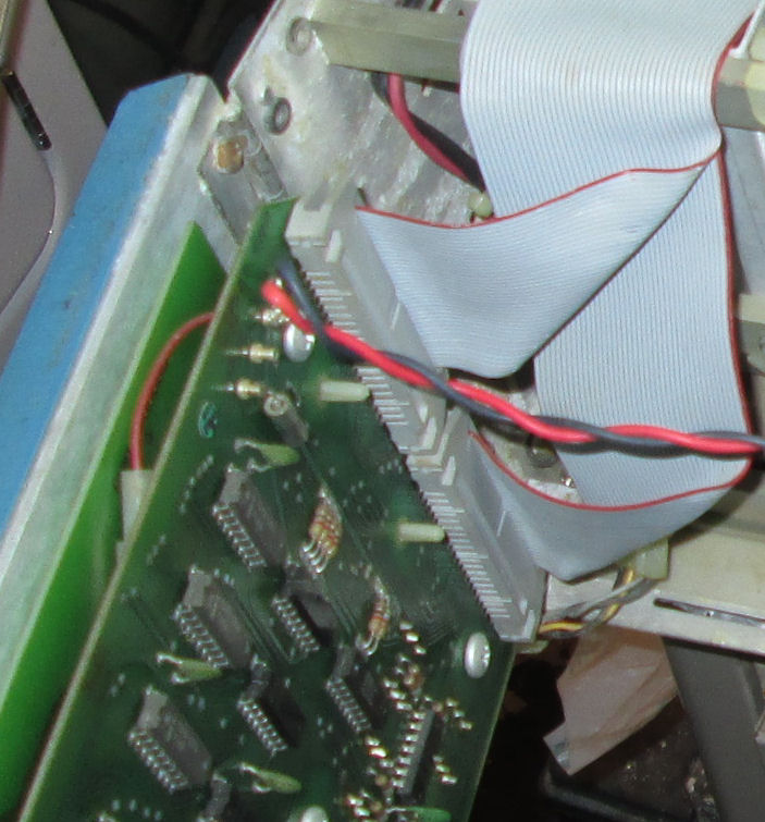
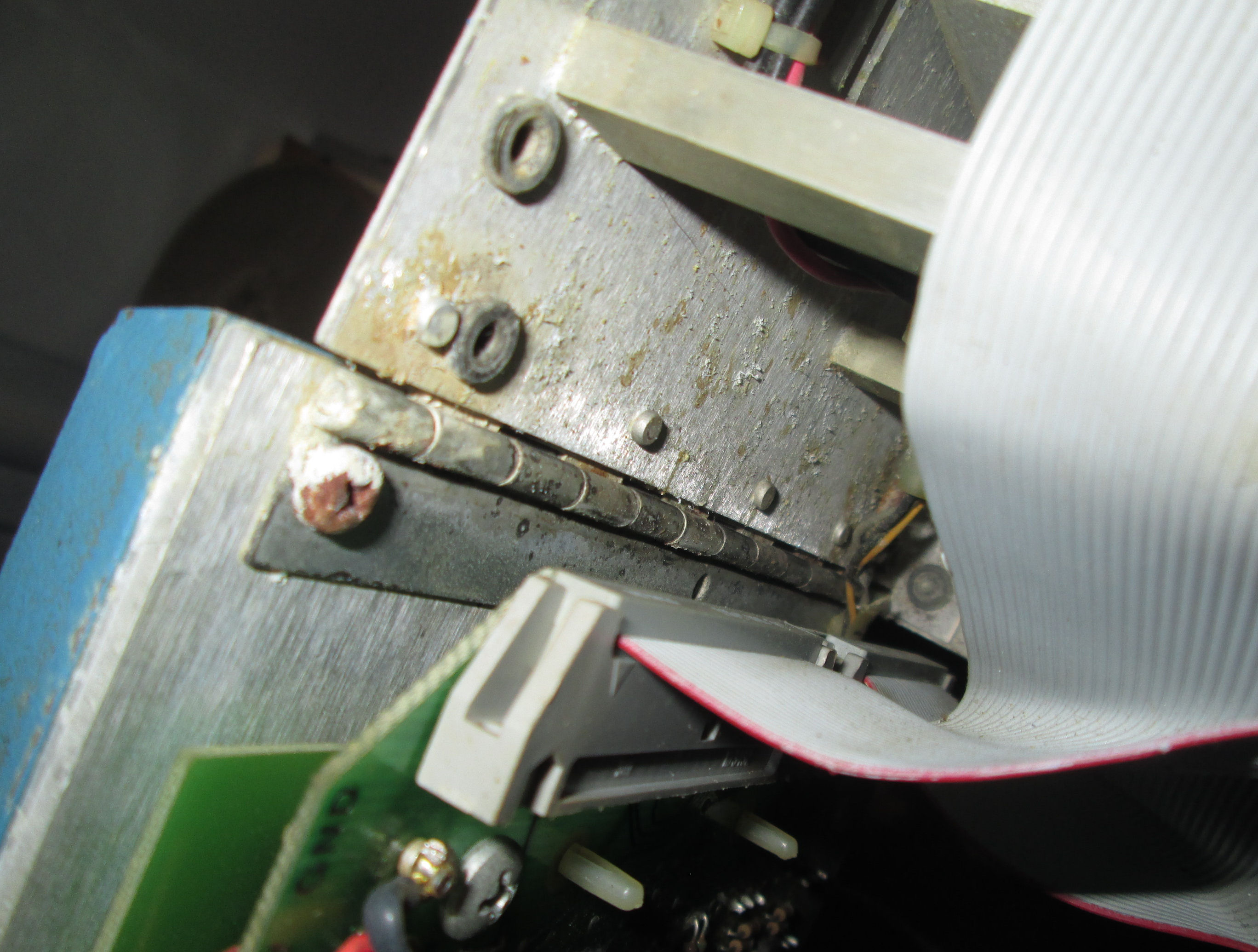
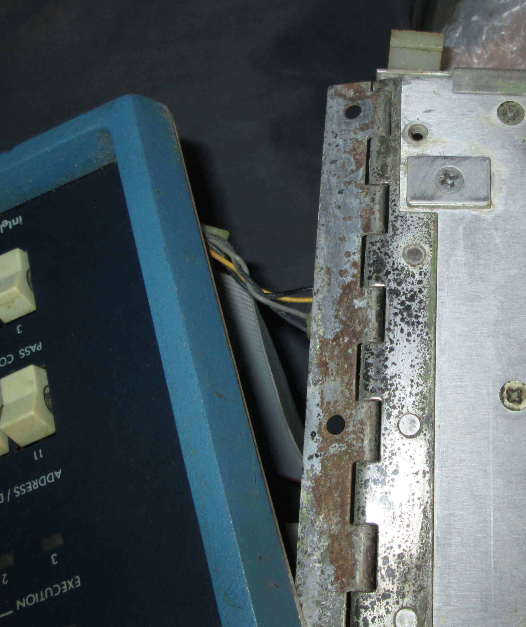
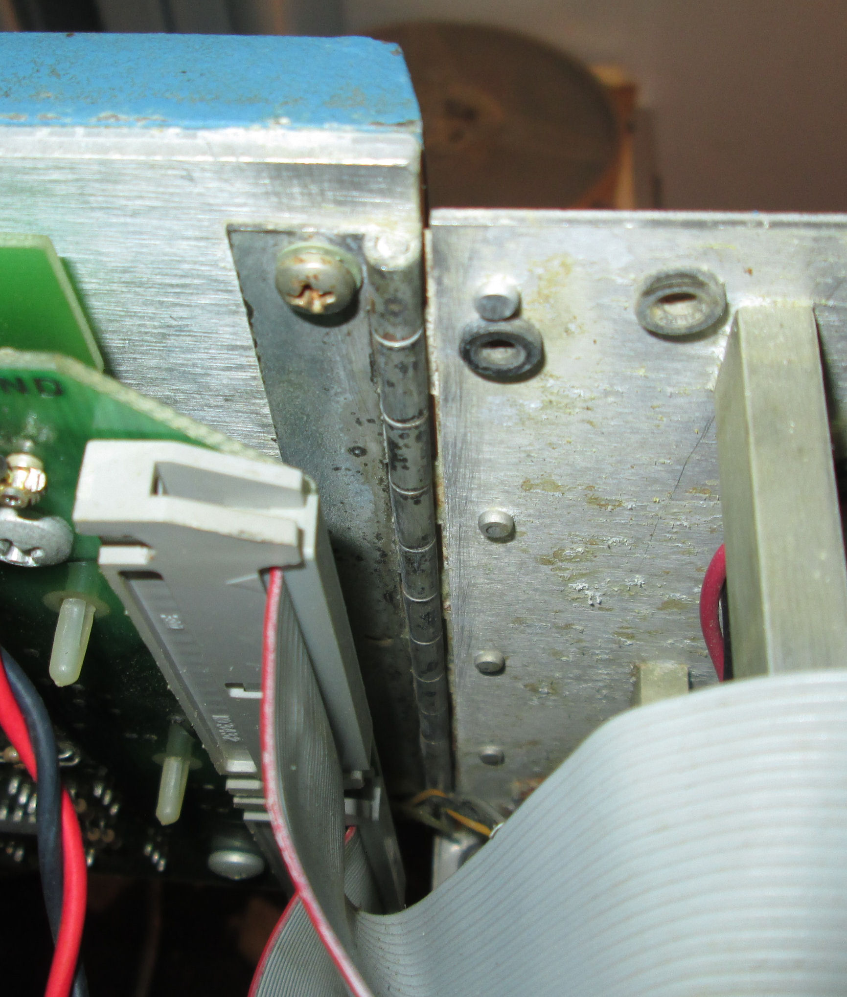
![[Intel MSC 4/40]](intel440_mcs_1.jpg) Here's the mcs intellec 4/40, viewed from the front panel.
Here's the mcs intellec 4/40, viewed from the front panel. ![[Intel MSC 4/40]](intel440_mcs_2.jpg) The 4/40, showing off the cards.
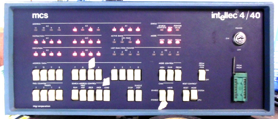
The 4/40, showing off the cards.![[Intel MSC 4/40 runs]](intel440_step.jpg)
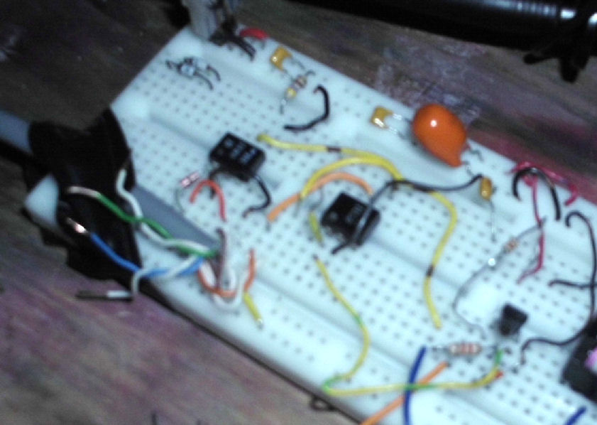
![[Intel MSC 4/40 interface]](440_serial_circuit4.jpg)
![[Intel MSC 4/40 screen]](440_serial_dump.jpg)