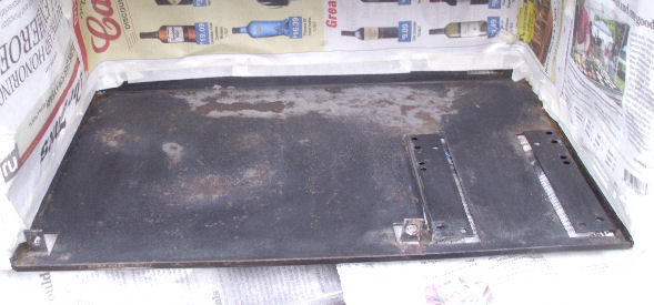
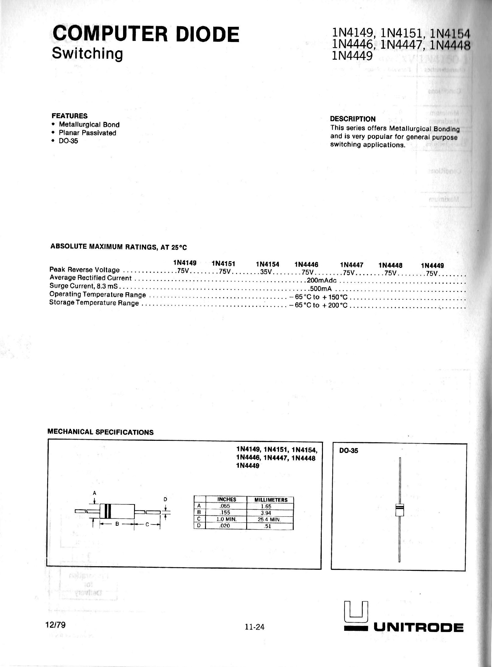
![[chassis before]](8a_recved_1.jpg)
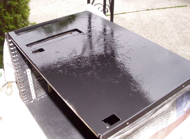
![[chassis after]](8a_1sttest_trans.jpg)
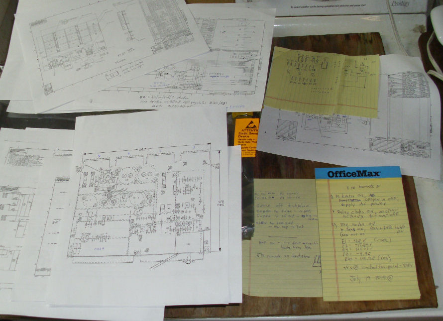
This Web page last updated date Oct 25 2019, link added May 14 2020. I obtained some PDP-8/A chassis and power parts in May 2015, examined and tested them and found some failures or issues. After some testing and small repairs I reassembled them. Took some time for me to get familiar with this DEC product's documentation and functions. After brief tests the power up and down operation and DC voltages look OK. In Sept 2015 I acquired a second power regulator and verified its DC voltages. That work is shown on this Web page. Next, I'll add the 8/A board set, and a DEC core memory, and a serial cable - these are first shown on this Web page, detailed elsewhere.
At the VCF-MidAtlantic repair event of Jan 29-30, 2016, I tested on a working 8/A: my 8/A board set, my core memory boards, and my programmer's panel. Then I assembled the best of these on my 8/A chassis, and ran tests with some success. Further work was done in early Feb 2016, to make sense of the M8317 bootstrap PROMS My thanks and great appreciation to David Gesswein, who provided total use of his 8/A, and patiently gave me instruction and answered questions; while he worked on another PDP-8. - Herb
And in Sept 2019, I did further work on the 8/A with some complete Programmers Panels at another VCF-MidAtlantic workshop.
In Sept 2019, I acquired another PDP-8/A system, and got some partial results. I'll make additional notes later but here's a stub about it.
See my other DEC minicomputers as listed on my DEC Web page.
Index of this Web page:
Notes on 8/A chassis repairs
2nd G8018 regulator, checked out
Other critical parts:
PDP 8/A board set
Core memory board sets
Programmers panel
Serial cable
8/A chassis Photos, detailing repair work:
photos of 8/A chassis "before"
photos of 8/A chassis "after"
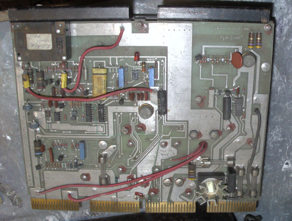
2nd G8018 regulator board & tests
Tech Notes:
Tech note: diode circuit analysis
Tech note: M8317 boot PROM notes
Other Web pages:
At the VCF repair event of Jan 29-30, 2016
See how I constructed a serial cable
Look at what I came up with for this 8/A programming panel.
to make sense of the M8317 bootstrap PROMS
To email me, see see my ordering Web page for my email addresses.
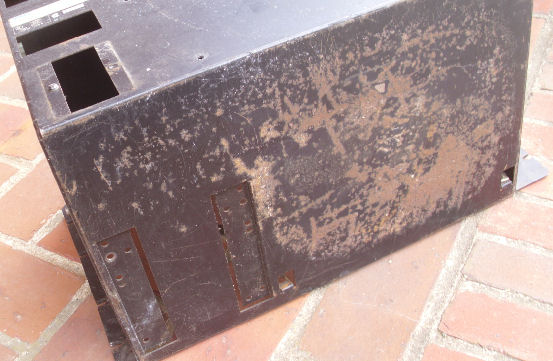
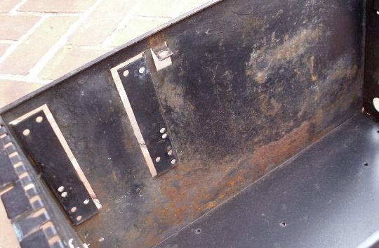
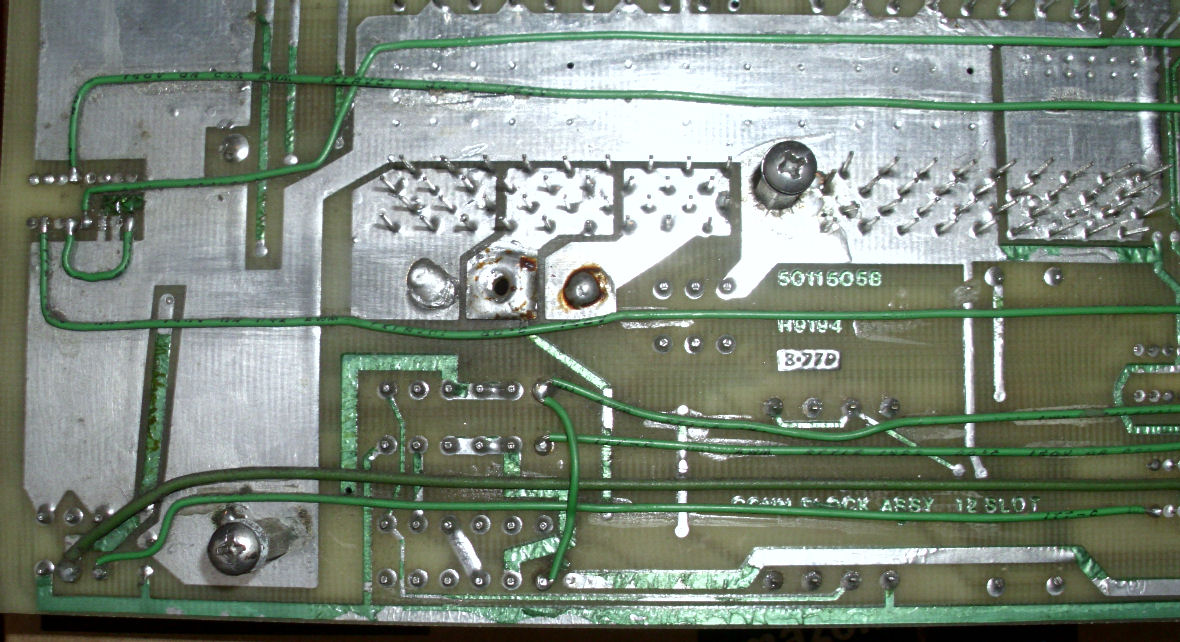
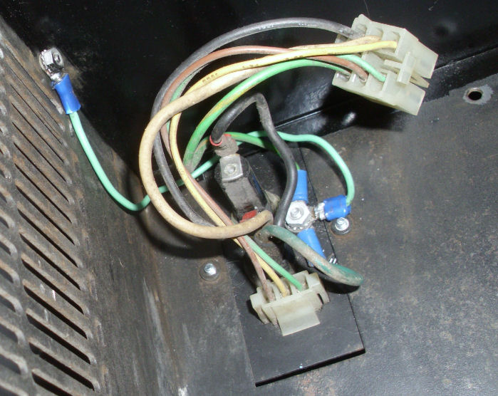
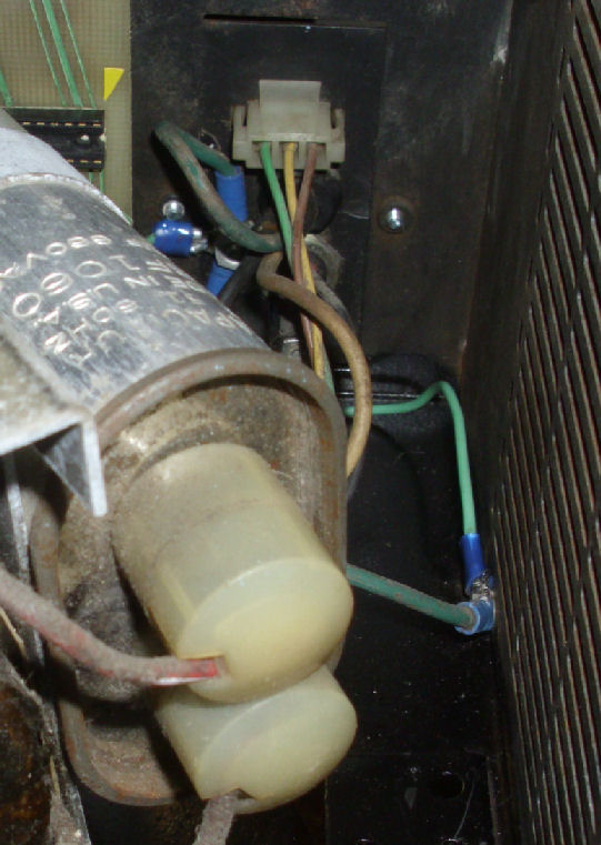
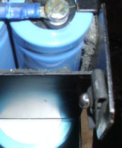
The 8/A chassis was recieved as a chassis with backplane, power regulator, transformer, and limited-function panel. There was some kind of power-up problem reported, but the G8018 power regulator and lim-fun panel were from a working 8/A system. The system was disassembled, examined and component level tested (mostly resistive and diode tests). DEC documentation from bitsavers was gathered and schematics compared to actual parts; some additional parts not in documentation were traced and schematics updated. A few parts were replaced; a cable connection was corrected. Part of the chassis was sanded to remove rust and repainted.
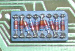
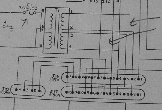
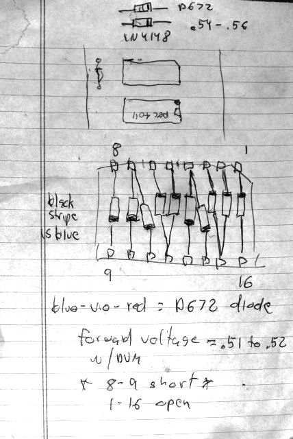
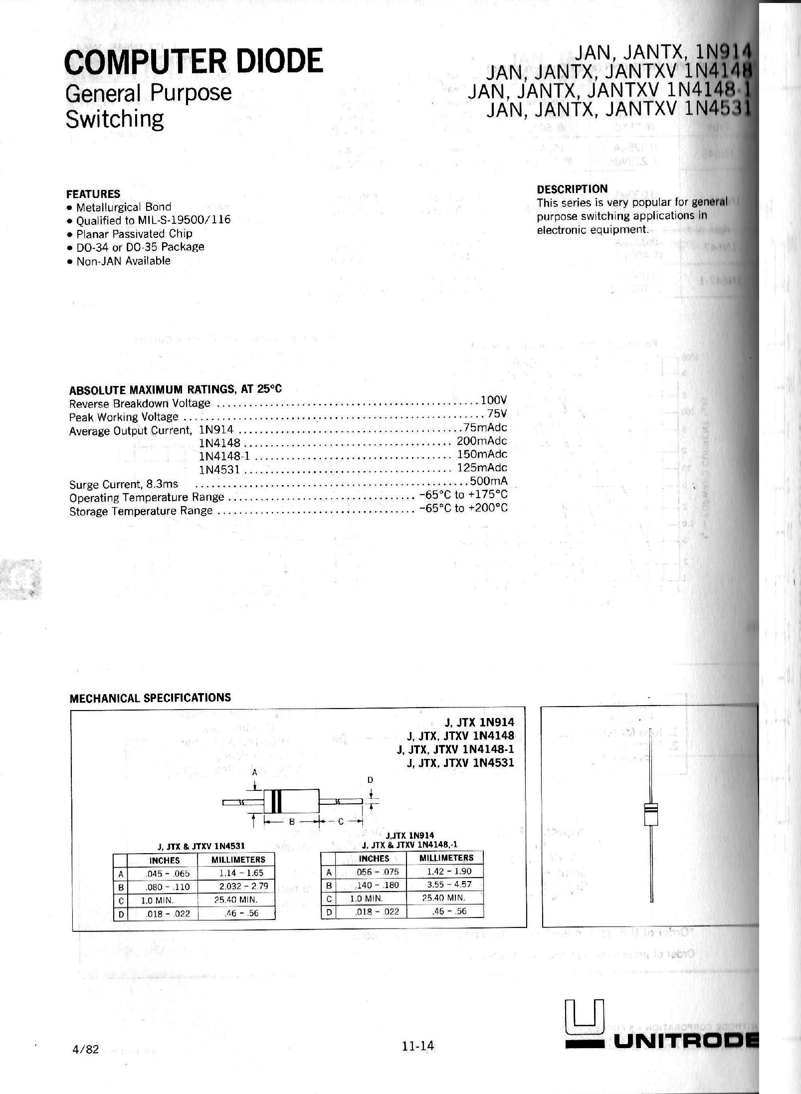
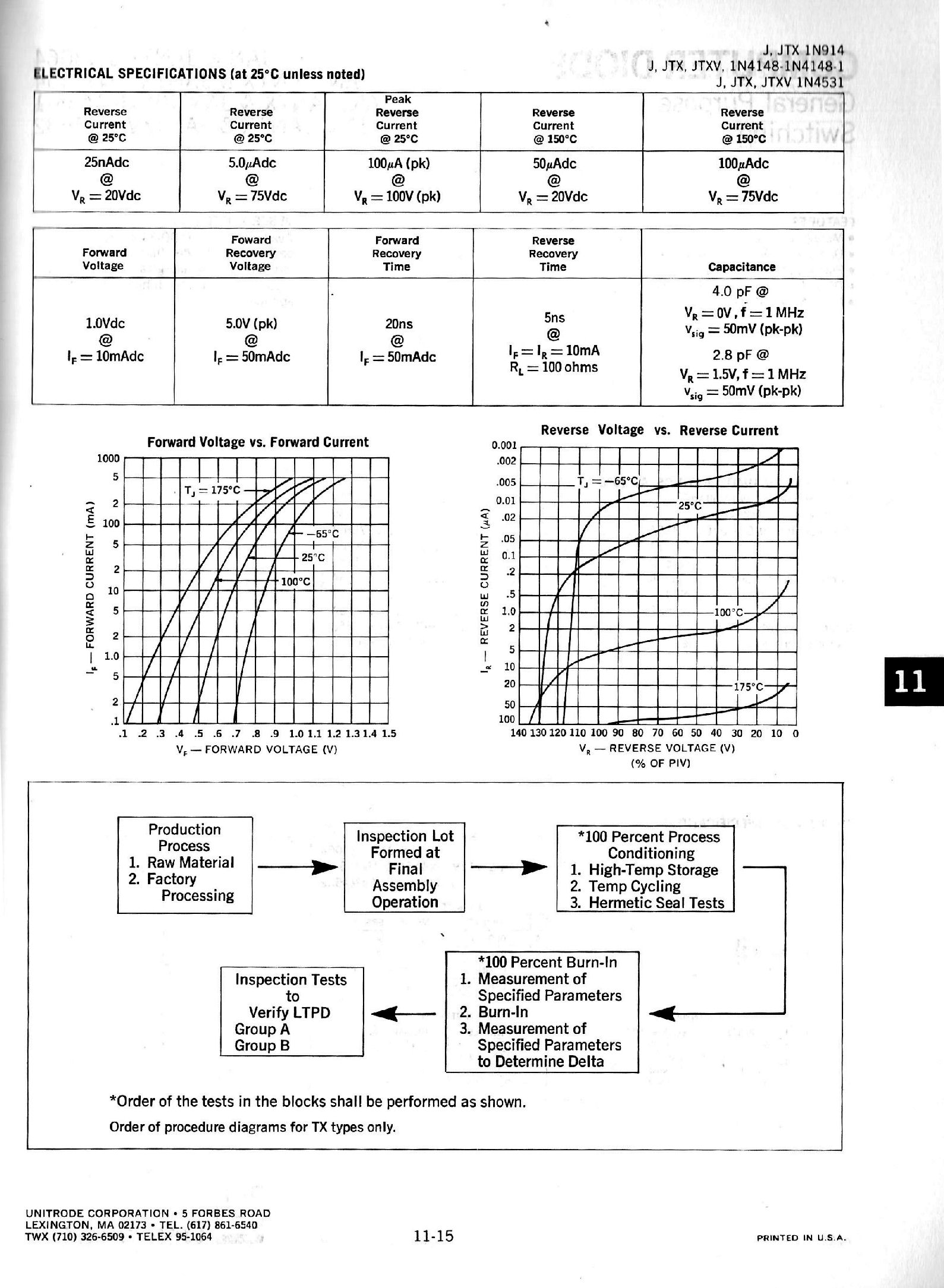
Two D672 diodes on the backplane diode header E2 were replaced with 1N4148's. 1-16 open, 8-9 shorted. These produce from the 5-volt AC windings, the POWER signal to the console connector J14 to the limited function control panel. See this linked analysis of the circuit.
The 3/8A fuse which was blown, was replaced. The limited-function panel DIP cable, was shipped with the cable DIP connected "upside down" on the backplane, cable draped down (toward base of transformer). I reinstalled cable "up", consistent with the DIP socket, and my trace of the backplane circuits and schematic.
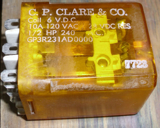
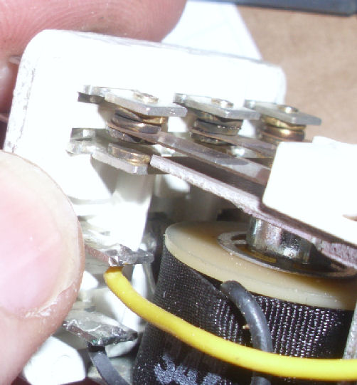
The backplane K1 relay contacts were dark; I filed them lightly. In the long run I'll see about replacing the relay or at least the contacts (using parts from a similar relay). The relay is a Clair GP3R231AD0000, 6V coil, 10A contacts.
![[tests]](8a_cab_paint1.jpg)
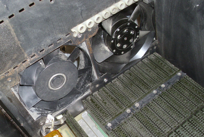
I added a second fan. I added various screws to mount items. Boards were lightly cleaned. The cabinet bottom, inside and out, was rusty; it was cleaned, sanded and repainted with epoxy paint. See my photos of the process. I added a ground wire from the AC cord panel ground, to chassis. (There's a transformer green wire also to the same chassis point.)
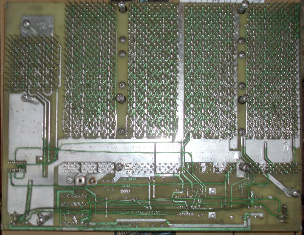
I spent some time checking the backplane for all the open traces versus the greenwire wiring - all "cuts" are covered. (I have an impression, this green-wiring was normal practice.) There were some components on the G8018 and the limited-function panel, not on my schematics: I traced and drew out the additional schematics for those circuits. I drew the component layout for the additional lim-fun panel components. See the photos for these revisions.
![[tests]](8a_1sttest_assembled.jpg)
results, first power, July 19 2015:, I reassembled the 8/A chassis from parts recieved, after repairs and cleaning. With no boards inserted except regulator and the limited-function panel, the chassis powered up with all DC voltages reasonable and fans on when the OFF/ON switch was ON. Testing was only for several minutes. Details of repairs and voltages read are below.
1) With DC breaker ON, lim-fun panel switch ON/OFF in OFF. AC power applied to AC cord. No AC voltage from chassis to AC plug ground. Result: relay "clicked" on. no other activity. This is normal.
2) as above, then ON/OFF switch toggled ON. Result: fans on. RUN and PWR lights on lim-fun panel on. LED D25 on regulator board on. Also normal.
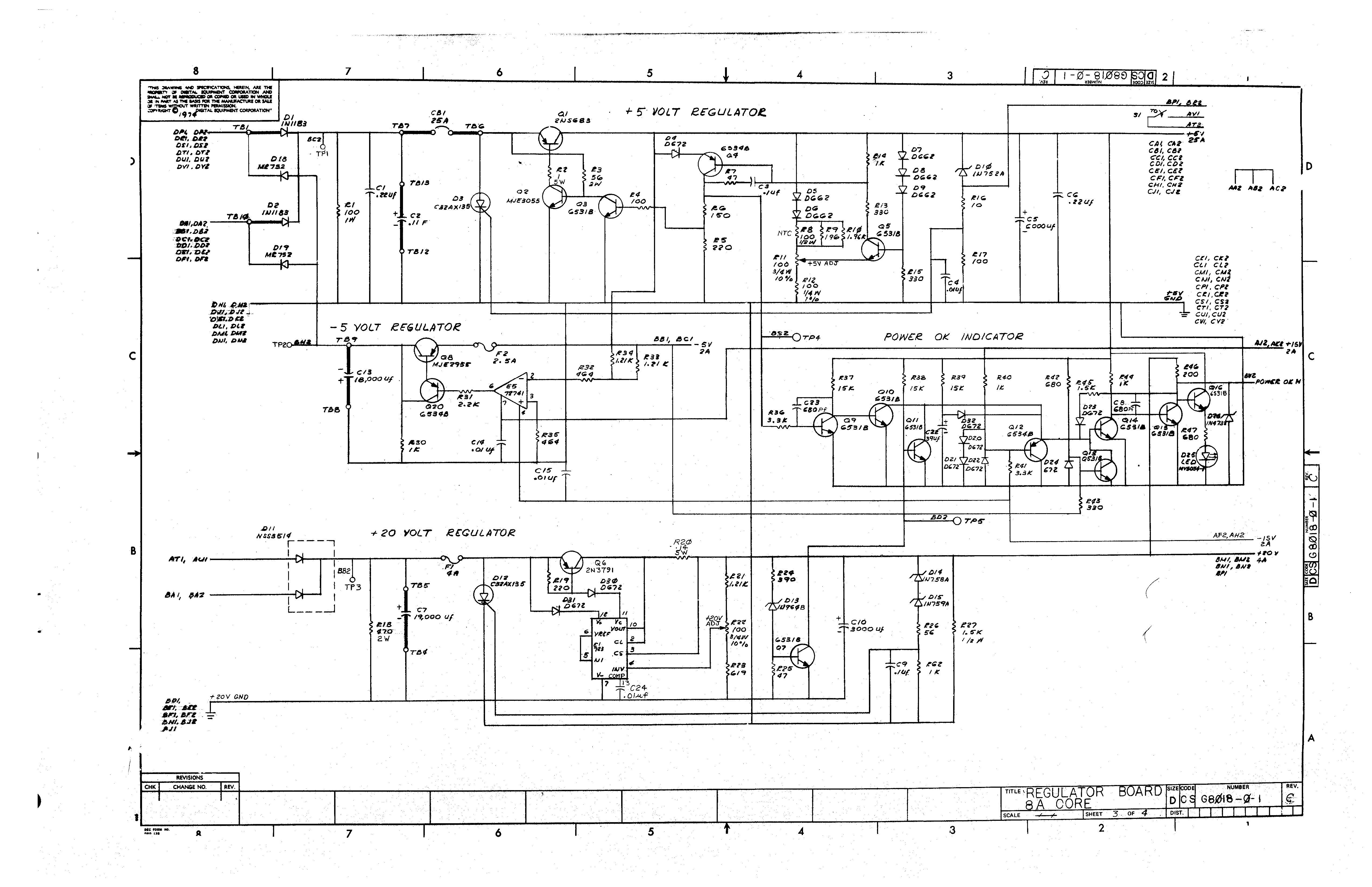
Voltages read on G8018, relative to chassis ground are:
at fuse F1 = 28V (unregulated +20V)
at fuse F2 = -4.96V (-5V supply)
at fuse F3 = -15.89V (-15V supply, no boards loading)
at fuse F4 = +15.73V (+15V supply, no boards loading)
at resistor R20 = +19.98V (regulated +20V supply)

At lim-fun panel I read +5V as +4.98V (+5V supply).
3) as above, then ON/OFF switch toggled OFF. Result: fans off, all LED lights off.
4) with AC power removed, relay clicks (presumably off).
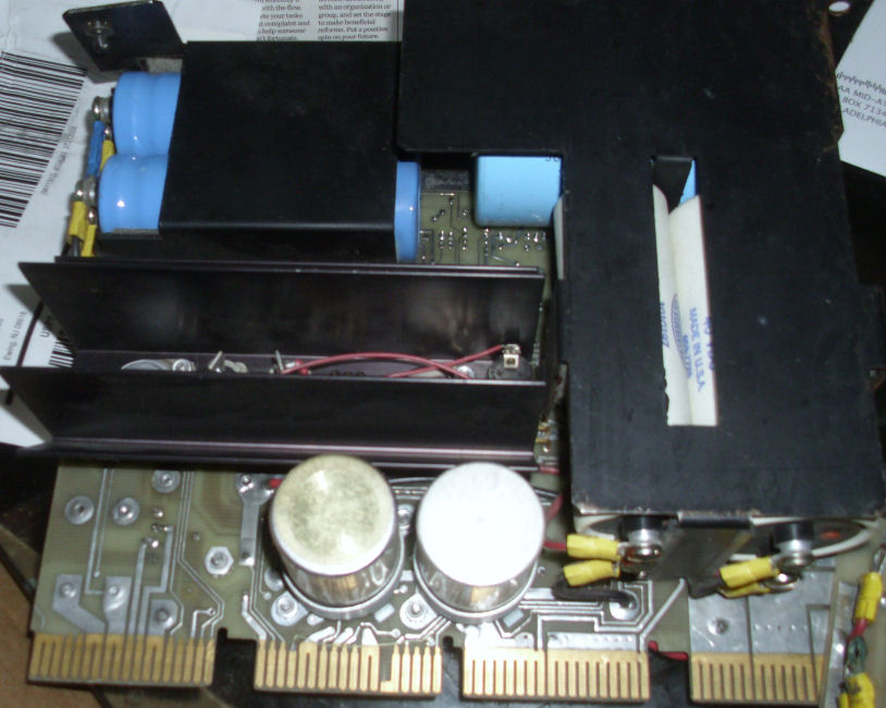
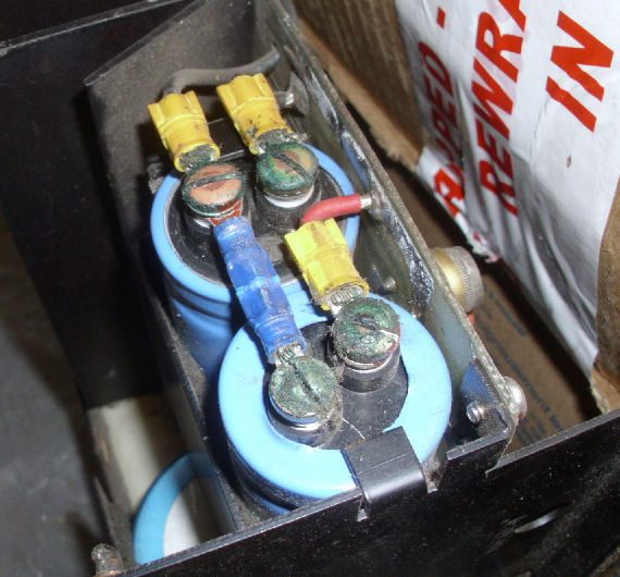
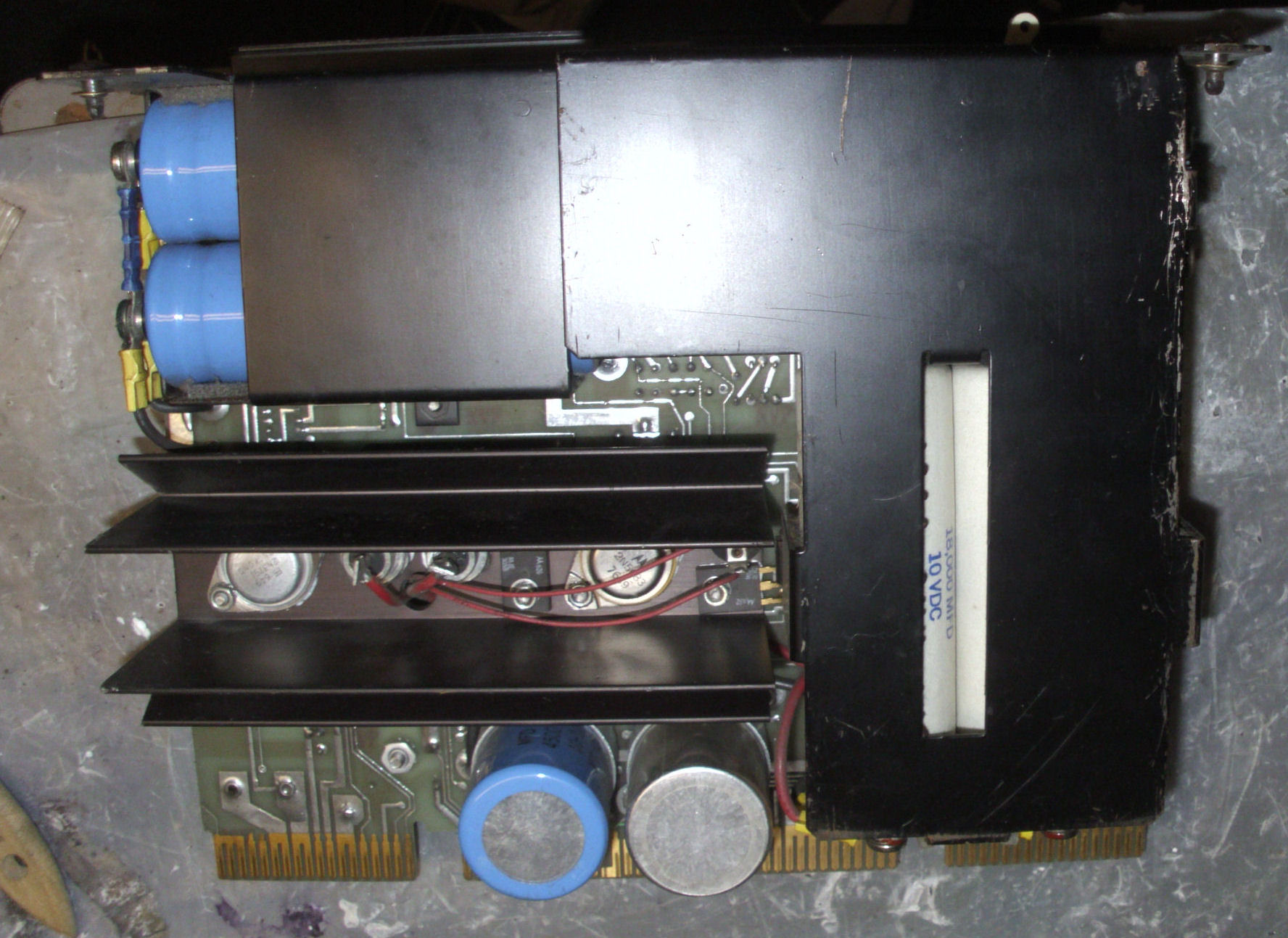
![[2nd G8018]](g8018_spare_2.jpg)
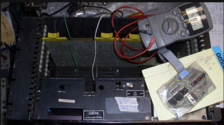
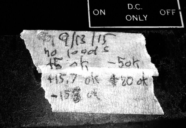
In August 2015, I had an opportunity to buy another G8018 in unknown condition at a good price. When it arrived it looked complete and had no obvious damage. The back looked OK as well. So I did some simple diode and transistor forward voltage tests. Most digital voltmeters have a "diode check" which applies and reads off a forward voltage drop across a diode or transistor junction. After reading off these voltages, I marked some suspecious transistors. Then I did the same tests between the "good" previously-recieved G8018 (right) and this 2nd "bad" G8018 (left).
I eventually decided the suspicious readings were likely due to circuit effects and not bad silicon; and I was reasonably satisfied
the power supply would not blow up under power. So I inserted the 2nd G8018 into the chassis and carefully did brief power cycles and quick checks of DC voltages. Most of the DC voltages are accessible from the fuse-holders, except +5V and +20 volts, which I read from
convenient components. When those tests showed reasonable voltages, I did longer runs with a 5-volt-only generic I/O card on the bus; just to load the +5V supply with something. 2nd G8018, DC voltages I read seemed reasonable and similar to the voltages read from the known-good M8018.
2nd M8018 voltages with modest +5V only load: +4.95V, +15.7V, -15.8V, -5V, +20V.
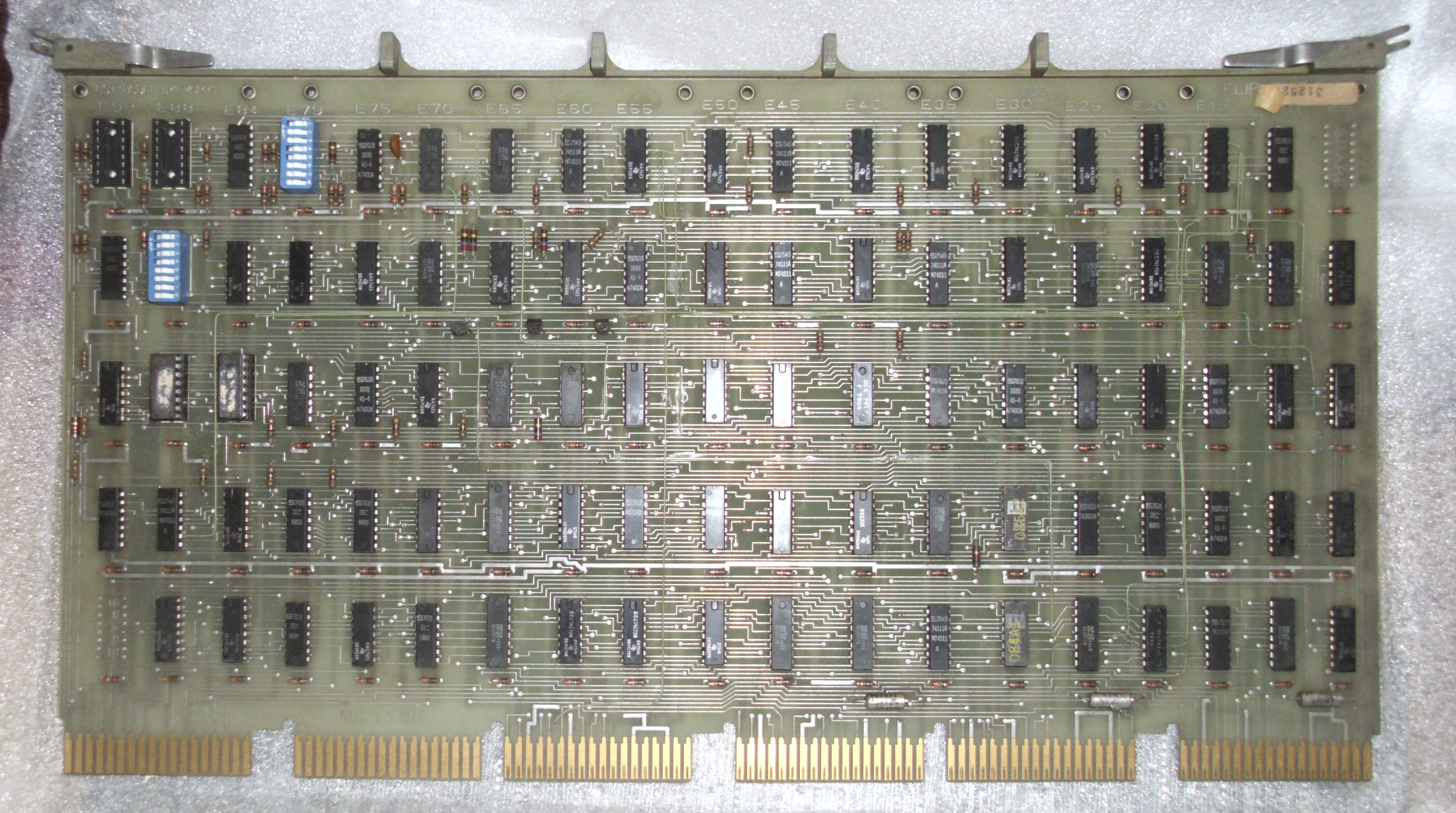
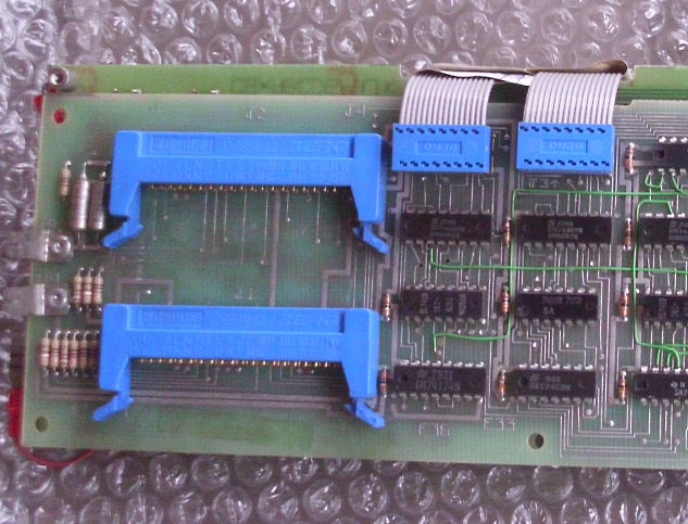
![[CPU 8/A]](8a_m8315.jpg)
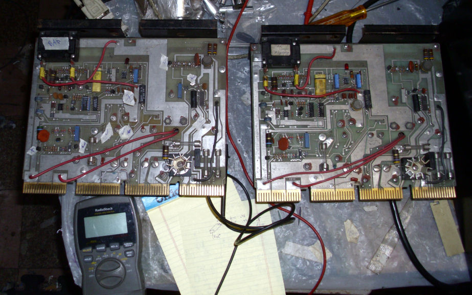
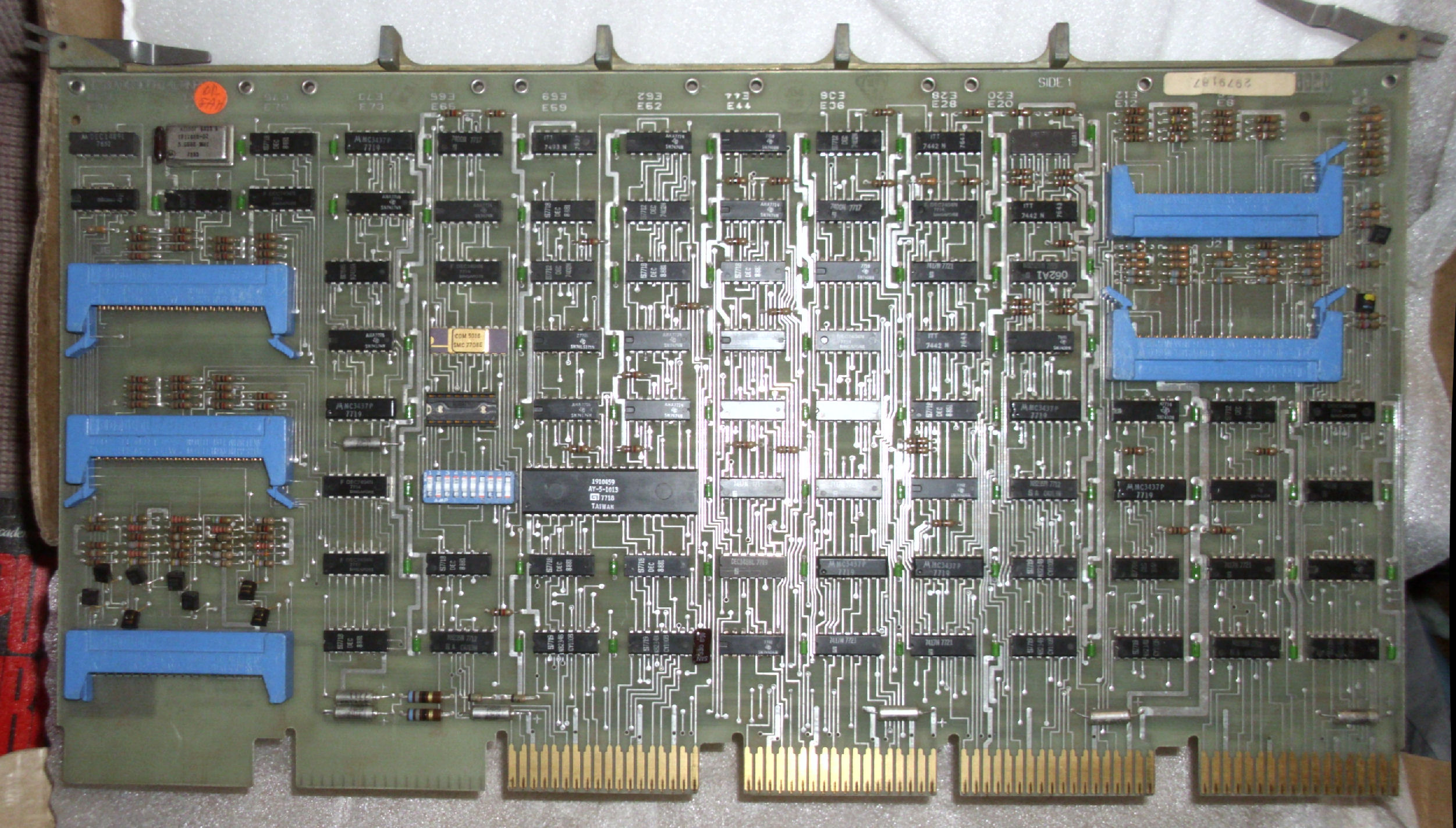
I purchased the 8/A board set below in 2014 as a tested and pulled set. I'll report results when I test them in the 8/A chassis. In May 2015 I obtained another M8315, which will need testing.
M8315, CPU, front view and no back view.
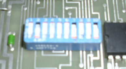
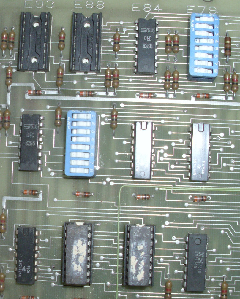
M8316, I/O multifunction, front view and M8316 switch settings.
M8317, Extended options, front view and M8317 switch settings and ROMS (lower center pair with damaged labels). This is not the -YB version.
What's on the boot PROMS? See my notes.
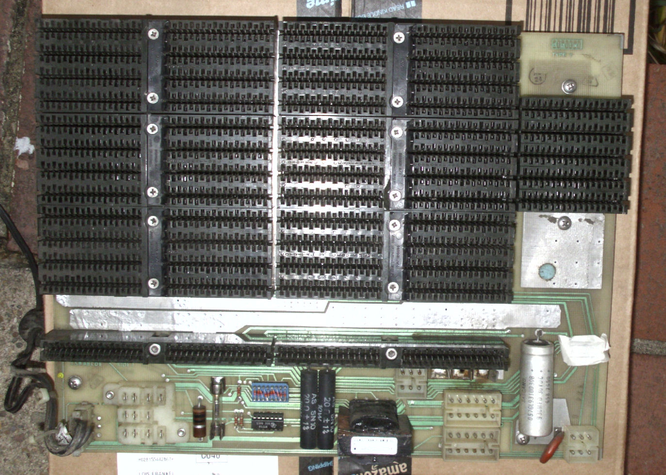
![[core 8/A]](G649.jpg)
I obtained the following core board pair in May 2009, as untested. a H219A core memory card s/n 7637-b-1406 etch 5010986B 5411531. Attached is G649 Core x-y driver & sense/inhibit card s/n 4541456. I'll refer to this board pair as "1406" after the core serial number.
In Jan 2016, I recieved two pairs of 8K core boards, as "these hang my system":
core H-219A S/N 7515- - -1489, etch 5010986B, 5411531
G649?, no lable
henceforth core-board pair "1489"
core H-219A S/N 7516- - -1613, etch 5010986A, H219
G649?, date 01/16/80, s/n M07110812
henceforth core-board pair "1613"
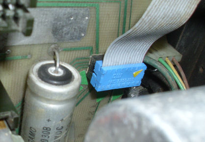
![[panel 8/A]](8a_prog_pan_0.jpg)
In 2015 Feb I obtained a two-board programmers panel set
- probably from an OEM PDP 8/A. Condition unknown. The back of the panel
has a pair of 40-pin flat-cable connectors back to
the M8316 I/O board; I can scrounge such cables. Eventually I'll have to do something with the
bare keypad. Look at what I came up with for this 8/A programming panel.
![[cable 8/A]](8aser_connect_fit.jpg)
For further repair work in Jan 2016, I needed to construct a serial cable assembly, from the
serial connector on the M8316 to an "EIA" serial connector DB-25. Rather than buy the correct parts,
I chose to cobble something up. But I think it will hold up for awhile.
See how I constructed a cable from convenient parts, and corrected a problem.
![[fix 8/A]](8a_fix_jan16_setup.jpg)
At the VCF repair event of Jan 29-30, 2016, I tested on a working 8/A: my 8/A board set, my core memory boards, and my programmer's panel. Then I assembled the best of these on my 8/A chassis, and ran tests with some success. Many thanks to David Gesswein, who
provided his PDP 8/A and assistance.
recieved cabinet
recieved backplane closeup
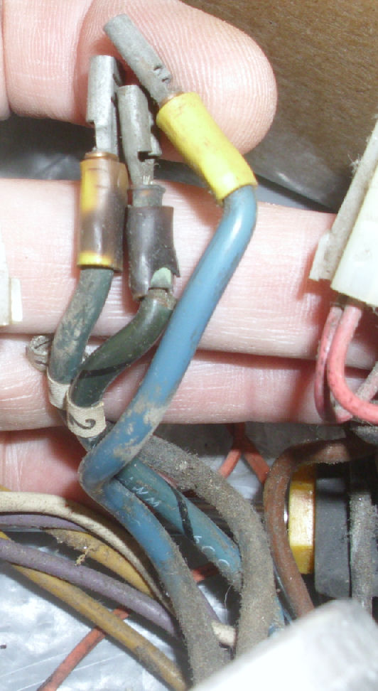
recieved transformer wires, lim fun panel cable
recieved trans wires and cotton dust
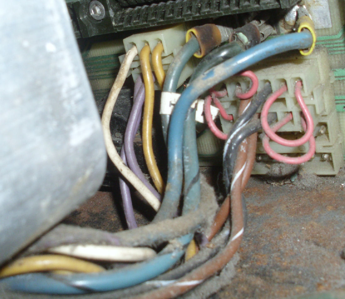
recieved G8018 cap terms, after some cleaning
recieved power trans
unsanded bottom of cab
unsanded inside cab
some sanding of inside cab and paint masking
painted inside cab with Rustoleum appliance epoxy paint
painted outside cab
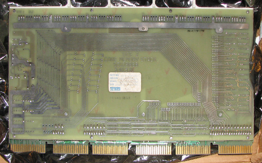
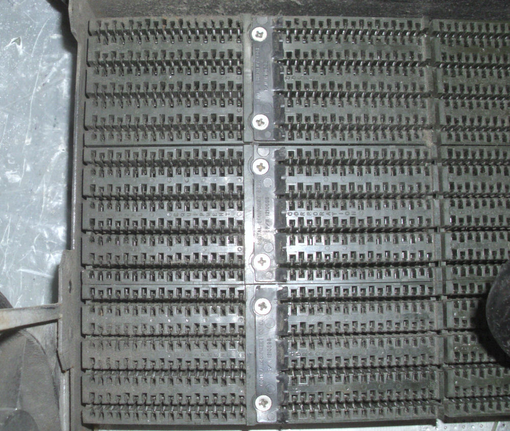
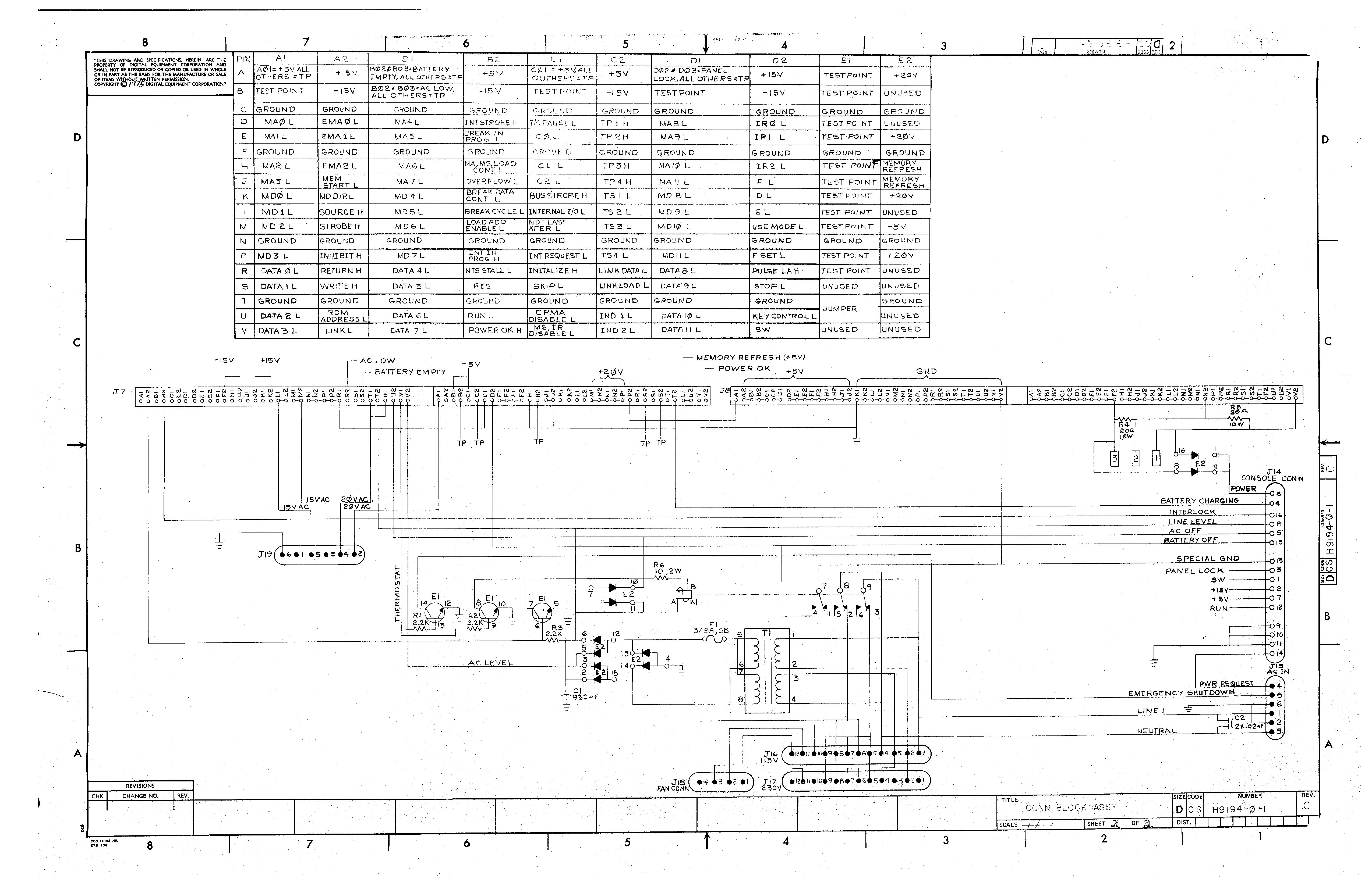
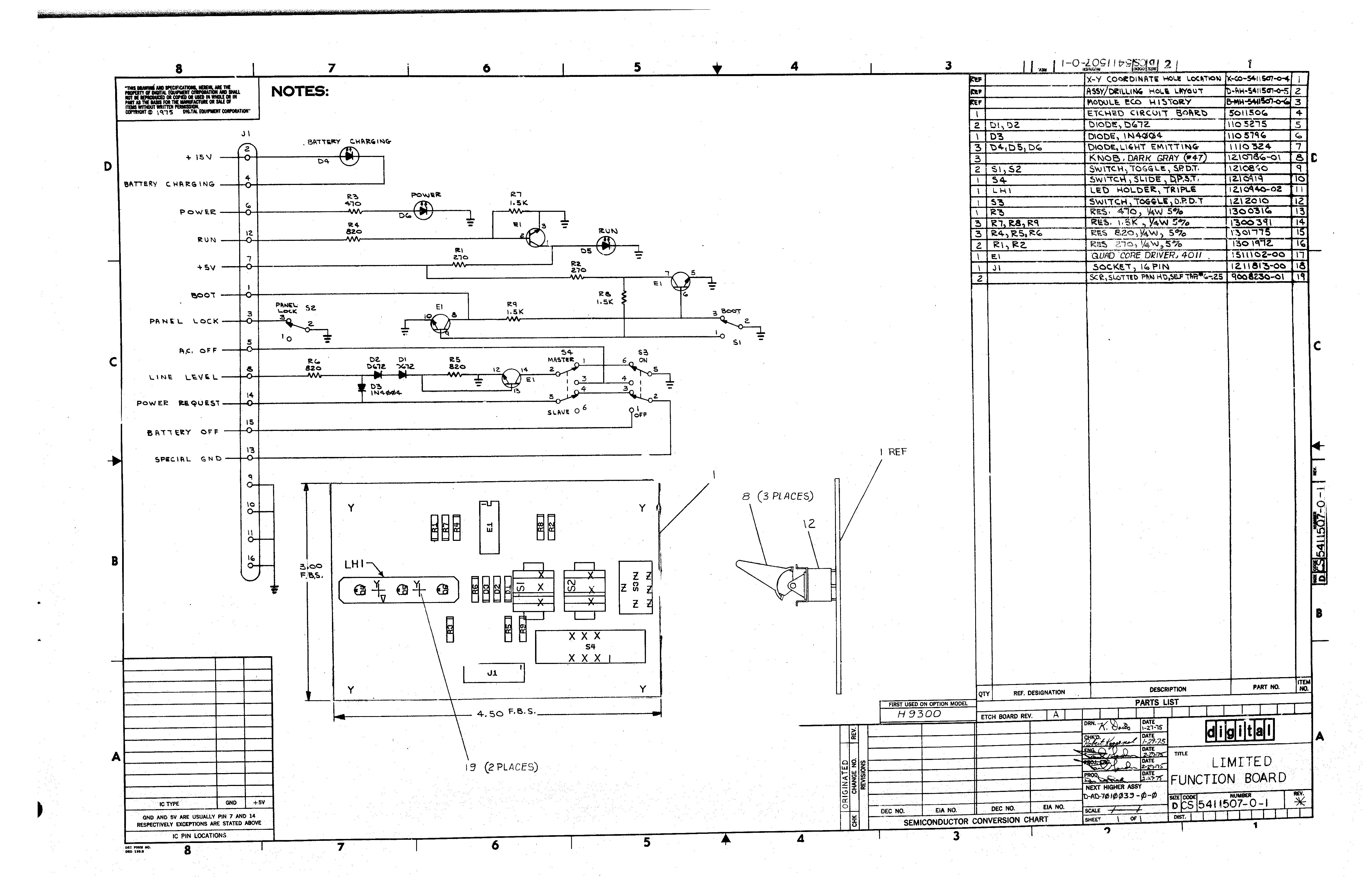
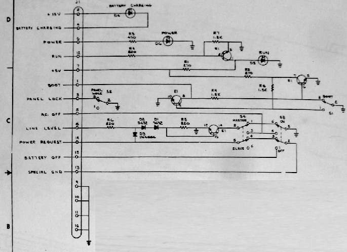
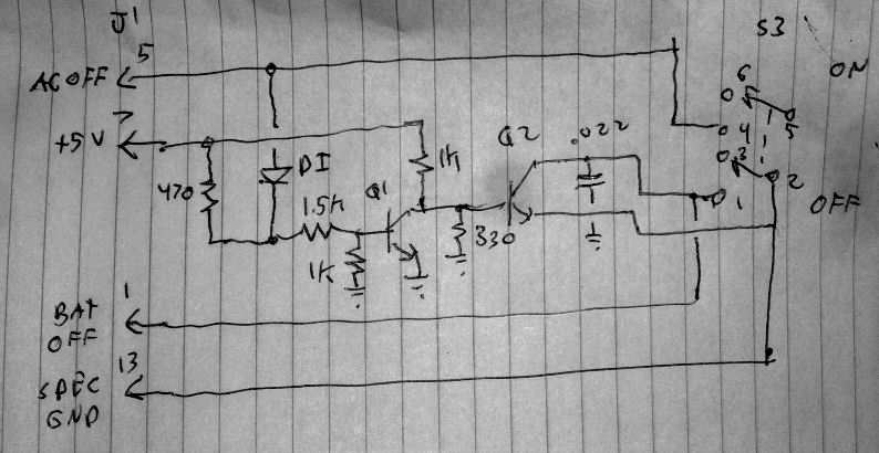
H9194 backplane schematic
H9194 backplane front
H9194 backplane back
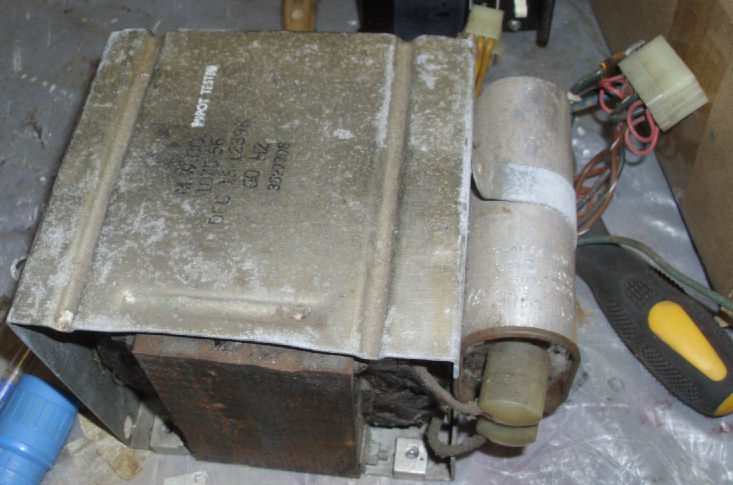
T1 transformer schematic primary windings indicate are about 400 ohms
power trans 123 leads removed
power trans 123 leads in place
green-wires to jumper PC board breaks
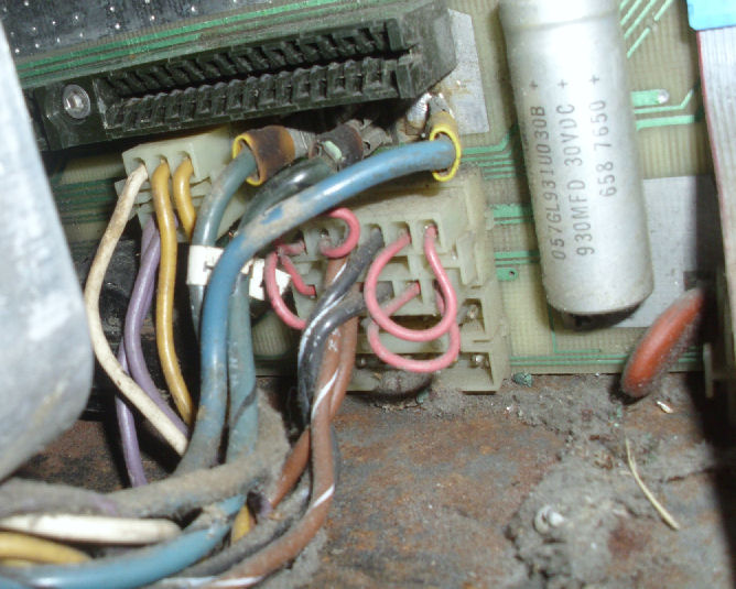
limited funct panel cable as should be placed. PC breaks marked to verify green-wired
limited funct panel DIP socket Note notch, pin 1 is upper right
relay contacts dark were cleaned with fine sandpaper
E2 diode header before repairs, in place on backplane
E2 diode D672 header layout and specs, broken diodes
replaced with 1N4148's. 1-16 open, 8-9 shorted, POWER signal to lim-fun panel.
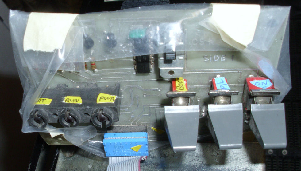
limited funct schematic and layout by DEC
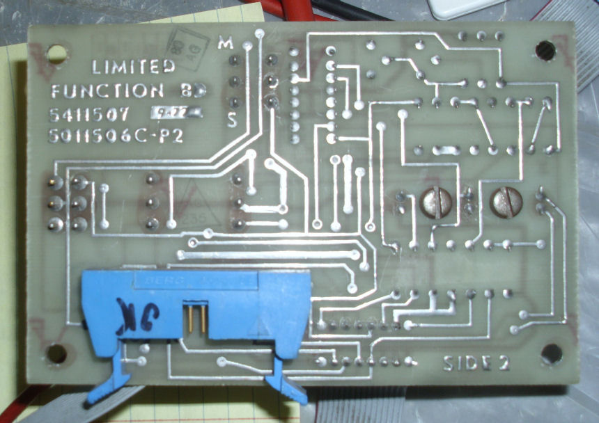
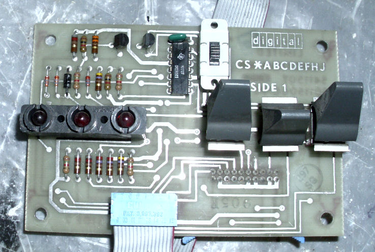
limited funct back
limited funct component side,compare to DEC layout to see additional parts
limited funct layout marked up
limited funct layout notes, parts not on DEC docs
limited funct sch from DEC
limited funct sch of additional parts
g8018 back side, heatsinks
g8018 top, component side
g8018 layout, DEC document
g8018 DEC layout closeup of board components
g8018 schematic 1 +5V, -5V, power OK, +20V
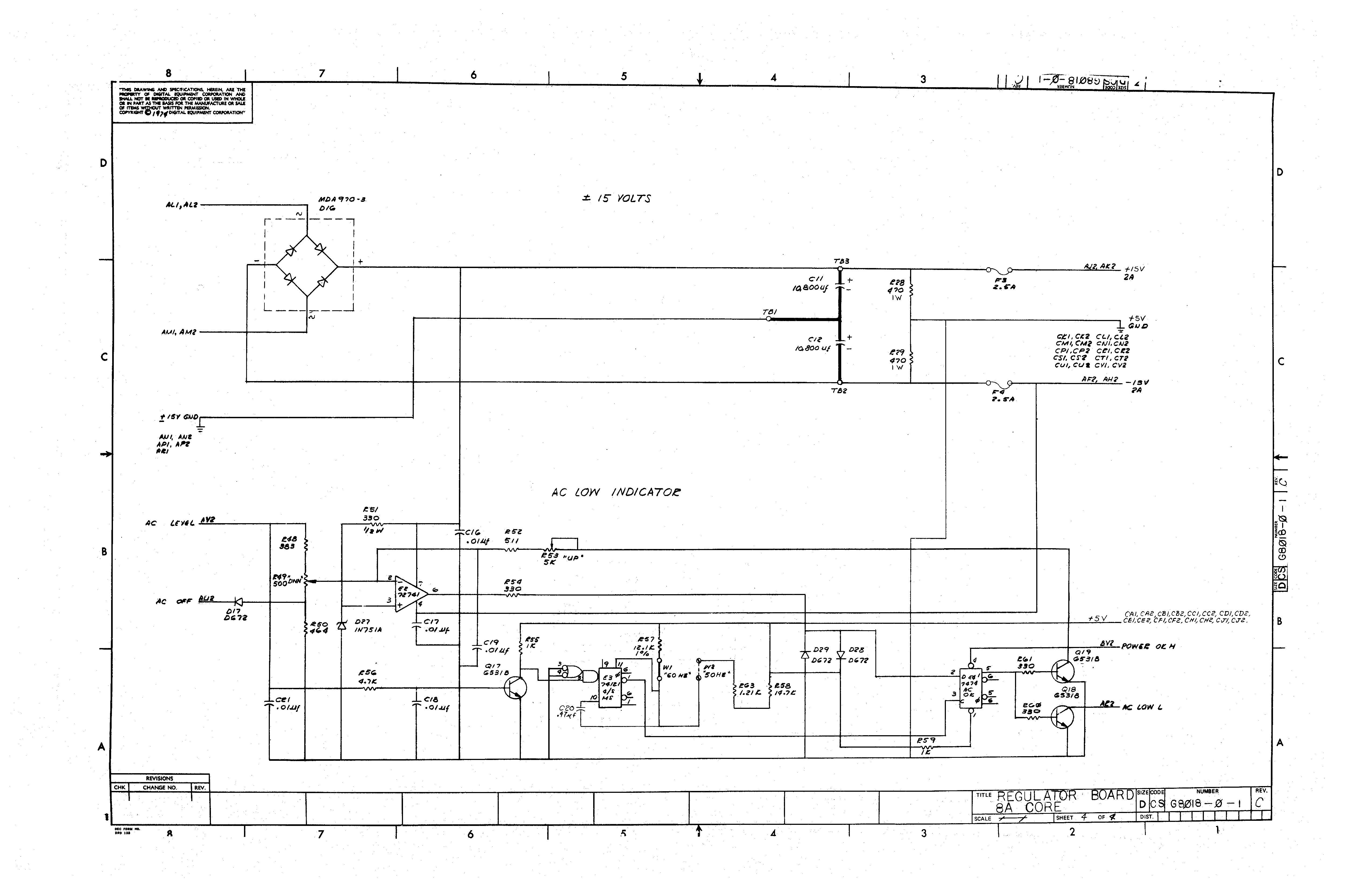
g8018 schematic 2 +15V and AC low
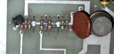
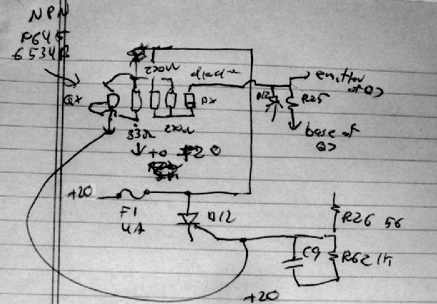
g8018 closeup, diodes and transistor not on DEC docs 20V regulator, D12 on right
partial layout of add'l 20V reg diodes, transistor
partial schematic of add'l 20v reg diodes, transistor
transformer and AC grounds to chassis
transformer and AC grounds to chassis
backplane and transformer placed
two fans installed
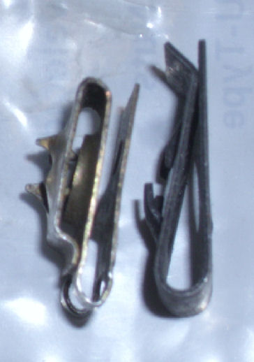
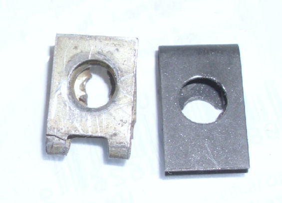
fastener to chassis, new in place
fastener to chassis, side view, original (grey) and newbie (black)
fastener to chassis, back view,
chassis, power supply, lim-fun panel assembled
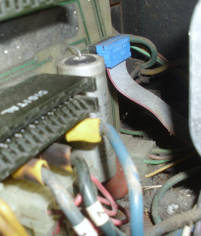
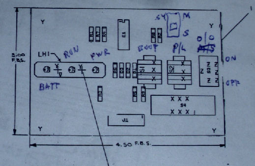
limited function panel, LEDs and toggles identified, insulated Note DIP cable pin 1 identified.
limited function panel on backplane NOte pin 1 identified.
schematic and layout notes prepared for testing
2nd G8018 power regulator board, unverified condition, heatsink side
2nd G8018 power regulator board, component side
"bad" G8018 on left, "good" on right - diode & transistor forward voltage tests, comparisions
2nd G8018, flagged diodes and transistors
2nd G8018, power testing, voltage checks
2nd G8018, DC voltages seem reasonable
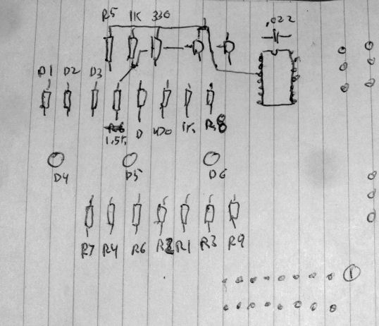
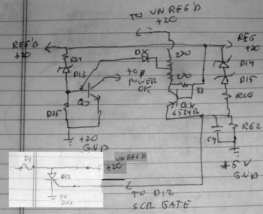
Vincent Slyngstad was kind enough to walk through the circuits to look at the use of the diodes, and confirm I could replace the DEC D672 diodes with more common 1N4148 diodes. His words are below, my edits are in []'s. - Herb Johnson
Looking at the schematics you sent, it looks like there are 4 pair of D672 diodes with shared anodes and one pair with shared cathode, "E2" in the H9194, and freestanding diodes D1 and D2 in the limited function panel.
If I am understanding the H9194 correctly, the common anode diodes with anodes at E2 pins 4, 12, and 15 are being used as rectifiers of a low frequency [60Hz] AC signal. The key design criteria there are probably max forward current (400 mA) and reverse voltage (75V, 100V peak).
[The pair at pins 5 and 3 produce a full-wave AC LEVEL signal to the regulator. The pair at 6 and 2 also has a DC capacitor to ground, and provides a LINE LEVEL signal to the limited function panel.]
Of the pair with anodes at pin 7, one half [at pin 11] is used to clamp the reverse spike from the relay, and the other [at pin 10] prevents AC OFF L from supplying current to the transistors. (Though I'm not sure why that would be an issue.)
The common cathode group E2 pins 16/1 and 8/9, also looks like a half-wave rectifier in the block diagram.[The pair of diodes on E2 pins 16/1 and 8/9, tap the +5V/-5V AC power transformer secondary windings connected at indicated tabs 1-2-3, which feeds the corresponding regulators. (On my system as recieved, one was shorted, the other open.) The diode common cathodes connects to J14 console pin 6 to create the POWER signal. That signal drives the POWER LED on the limited-funct panel.]
That leaves D1 and D2 of the limited function panel [on the LINE LEVEL signal]. Those do seem to be quite different, and definitely using the forward drop to affect the transistor bias at E1 pin 13. It looks like the current through the 820 ohm R6 is meant to drop all but 3 diode drops worth of voltage, and then two more D672 drops is supposed to bring E1 pin 13 to the base-emitter forward drop of E1. Or maybe the way to think about it is that LINE LEVEL is divided across the 820 ohm R5 and R6, but is offset by D1 and D2, then clamped by E1. Looked at that way, there is likely plenty of bias current as long as one half of LINE LEVEL is more than the three diode drops taken together.
Looking at the regulator card schematics, I see that LINE LEVEL is attenuated by some resistors and compared to a 5V reference level to detect AC LOW. The attenuation is adjustable from .4X to .5X, so I infer the normal value of LINE LEVEL at a 95V line level is near 10V. Normal operation is probably a little higher, 11 or 12V.
That seems to indicate that the limited function panel will work OK with most common diodes as D1 and D2.
diode technical data
Diode data
1N4148_1 spec
1N4148_2 spec
1N4149_1 spec
1N4149_2 spec
Gotta figure out what bootstrap ROM set is in the M8317, with its 128 instructions; or more likely burn replacements. However, these boards were from an OEM 8/A, and it may have booted a custom cassette drive, so the ROMS in there may be irrelevant. The ROMS are two small fuse-link bipolar devices, 256 X 4 bits. I"ll discuss how to read and possibly replace them in these notes.
note: I'm generally interested in old bipolar PROMS, which were also used in early microcomputers of the 1970's. For more information about bipolar fusable PROMS in vintage computers, check this linked Web page where I show several examples and how-to-read and program them.
Reading the DEC schematics... 23-0008A is DEC's unprogrammed part number, 256 X 4 each, 16 pins. ROMs #1 E82 and #2 E87 (socketed) have these pinouts. Address lines 1-7 and 15, data lines 9-12, 13 and 14 some kind of active-low select. There are 1K pullup resistors on them, this suggests open-collector outputs. Addressed in pairs they provide 12 bits of instruction and 4 bits of extended addressing. Programmed DEC versions may be part number 23-087A2, 23-088A2.
There's also soldered-in PROMs at M8317 board location E26 (32 X 8, 23-084A1) and E27 (256 X 4, 23-086A2). My photo shows those 086* part numbers in yellow, and show these are MMI brand parts. These are likely used for logic, not code. In a similar way, on the M8315 (CPU board), DEC's programmed PROMS are also used for instruction decoding. They are mostly 256 X 4 but one is 1024 X 4,.
On the M8317 boot PROMs again: DM74S387 or DM54S387 has the same addressing pins, the same data pins, the same active-low selects. Unprogrammed the outputs are low. When the two selects are low, the open-collector outputs (74S387) go loose (pulled high by resistors), the tristate outputs (74S287) go high-impedance.
From the Operator's Handbook: "There are three types of bootstrap ROMs used on the KM8-A. E82 and E87 have different labels for the different bootstrap ROMs. Switches on modules that have E82 and E87 (Figure 3-16) labeled 87A2 and 88A2 should be set according to Table 3-11. If E82 and E87 are labeled 158A2 and 159A2, use Table 3-12 for switch settings. For CL8 systems using the RX8-E, E82 and E87 are labeled 156A2 and 157A2; use Table 3-13. (If Table 3-13 is used, Auto-Restart address must be selected, i.e., S2-2 is OFF, S2-3 is OFF, and S2-4 is OFF.) "
Further work was done in early Feb 2016, to make sense of the M8317 bootstrap PROMS. My thanks again to David Gesswein for providing ROM dumps of his 8/A and offering to copy ancient TTL PROMs.
From Mike's Arcade at http://www.mikesarcade.com find the list below. Seems these PROMS have the same pinouts and are either tristate TS or open collector OC. Unprogrammed prices seem to be undr $10 each. Jameco, Electronic Surplus, hobbyroms.com, arcadecomponents.com, eBay of course has some of these. Some sellers offer programming.
V1.6 Jan 13,1999
Fujitsu
-------
                 SIG     AMD    MMI      NAT    TI      HAR     FAR
7113 256x4 OC == 82S126, 27S20, 6300,   74S387, 24SA10, 7610
7114 256x4 TS == 82S129, 27S21, 6301,   74S287, 24S10,  7611, 93427