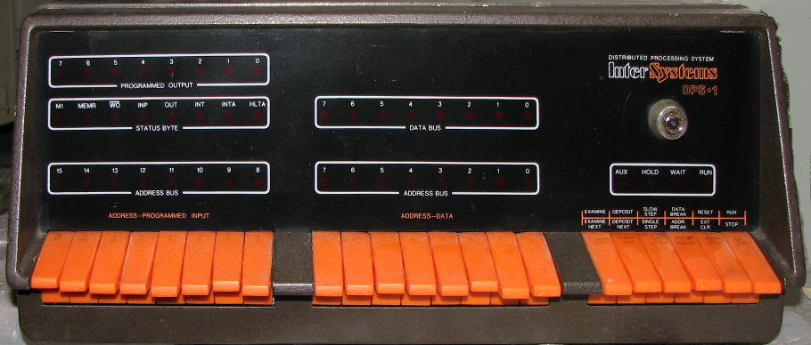
![[Ithaca DPS-1]](ith_cleaned.jpg)
Last update April 3 2016. This Web page originated Nov 26 2009, with content added July 13 2012; July 23 2013. Work restarted Mar-Apr 2016. It is part of a number of repair and restoration Web pages I have which are linked from this Web page My S-100 Web pages have a home at this Web link. I have an Ithaca Intersystems Web page at this link..
I started work on this Ithaca Intersystems DPS-1 system in early September 2009. On this Web page, you'll see how I cleaned it up, worked from the CPU and front panel to get the two functioning, and then added and tested the remaining cards, and a few diskettes. I had a failure - blown fuse, damages - which I fixed. It still had problems, and I put it aside. See how I made progress, false leads, blind alleys and all! Failures are more educational than successes, you know.
In June 2012 I was asked about the C&K toggle switches on the front panel so I took some photos, and had an extended discussion with Kip Yeakel. He came up with recent C&K part numbers to obtain Ithaca-compatible front panel switches, to match the FP card and paddles he obtained recently. Details are on another Web page but the numbers and summary are here.
Later I worked on some Ithaca boot system disks, but this work may not have produced working disks (I learned later).
In Feb-Mar 2016, I worked on another DPS-1 system and actually got that one working!. Check out my work on that other DPS-1 system on this linked Web page. With that working system and worked-on Ithaca boards, I could test another set of further and get a second working set, to run in this DPS-1 front-panel S-100 mainframe. Details would overwhelm this already large Web page, so please look at my Web page on my 2016 repairs of this chassis, which I started work on in 2009.
- Herb Johnson
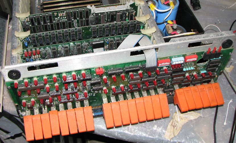
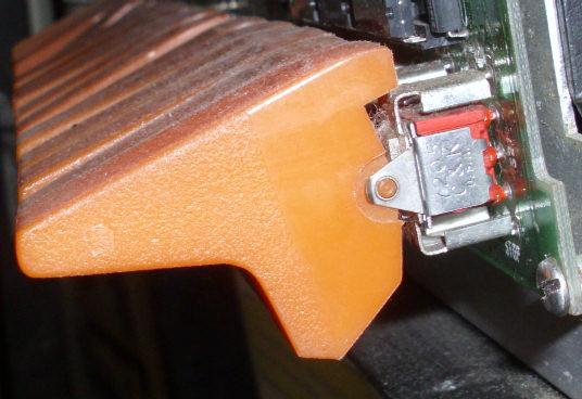
The photo above shows the DPS-1 with its distinctive front panel of orange switches.
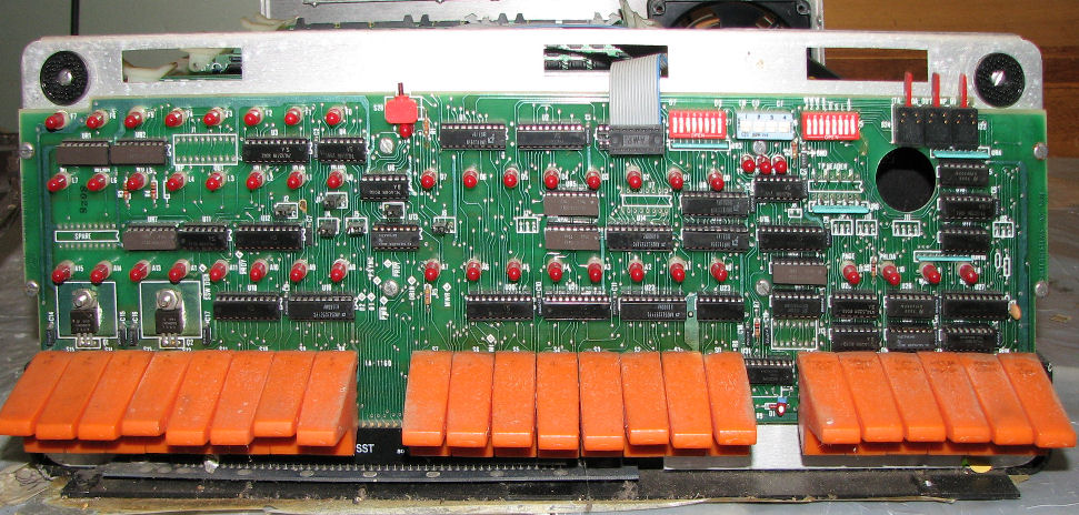
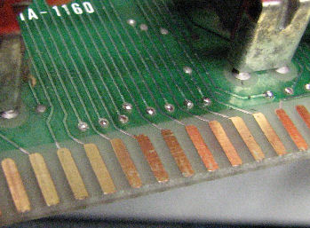
IA-1160 front panel board
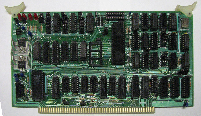
IA-1020 "Z80 II" CPU card
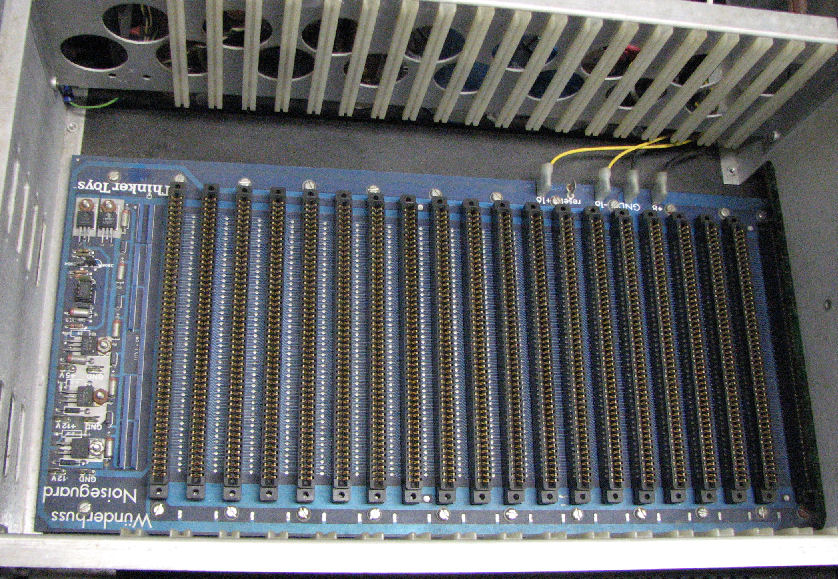
Thinker Toys Wunderbuss motherboard with active terminator
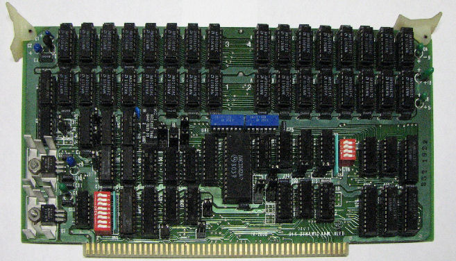
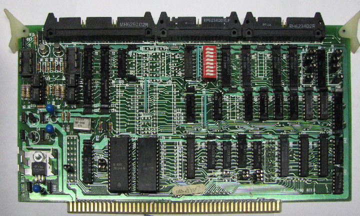
one of two IA-2030 64K DRAM cards
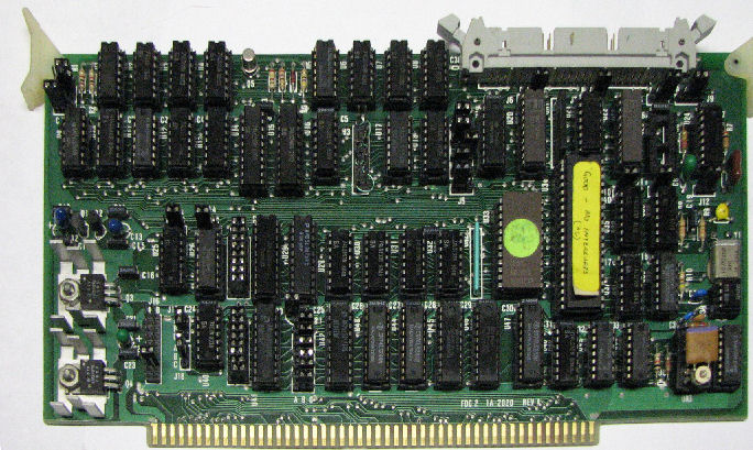
IA-2020 FDC-2 card
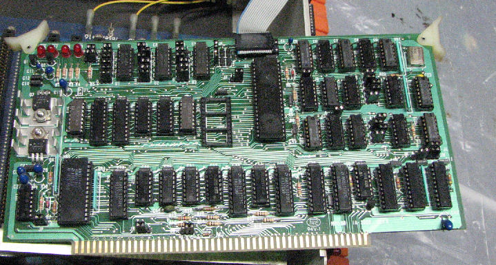
IA-1190 VIO I/O card
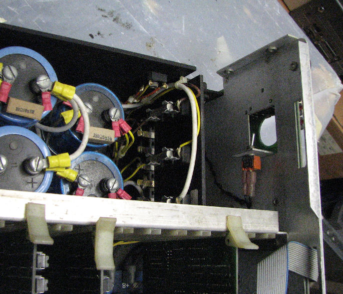
front of Ithaca power supply, +18V -18V caps, fuse panel
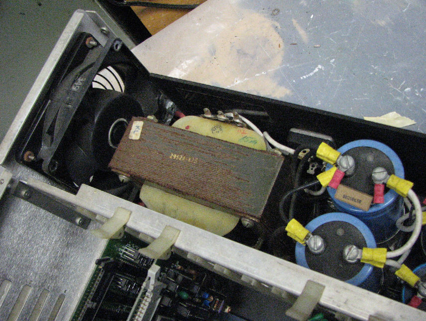
rear of Ithaca power supply, fan and transformer, +8V caps
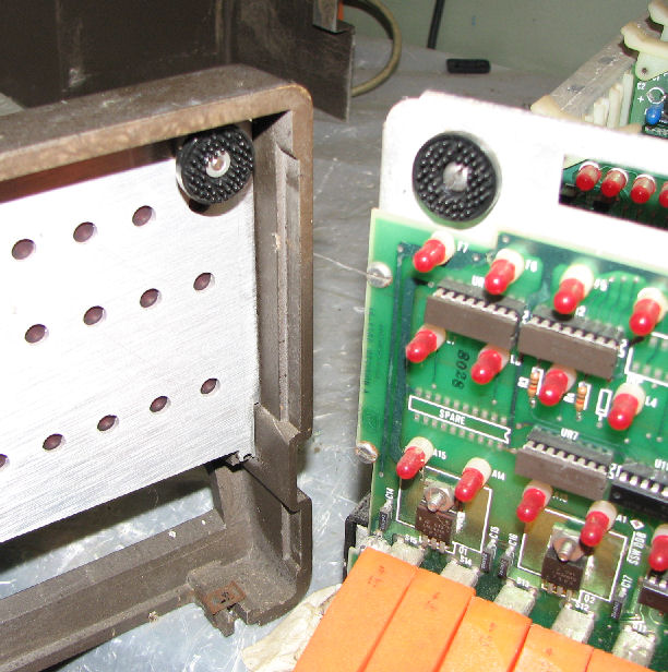
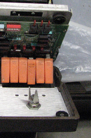
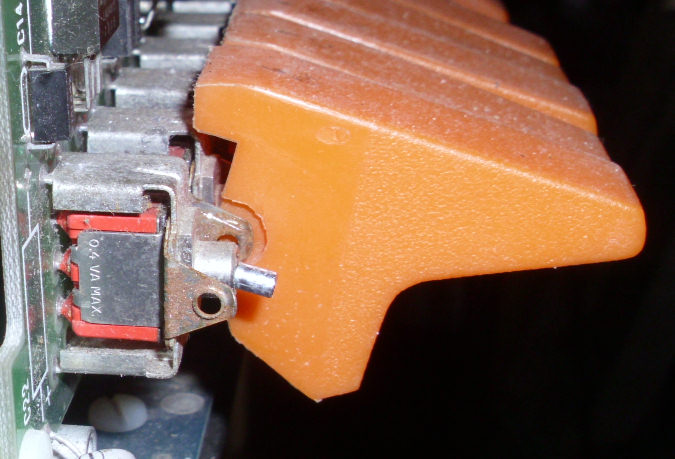
The front panel cover is held with Velcro catches between the front of the chassis and the back of the front cover. See how the front of the power supply includes the AC power switch , which is access through a hole in the front panel logic board. The front cover key switch from rear rotates to toggle the power switch, through the hole in the board.
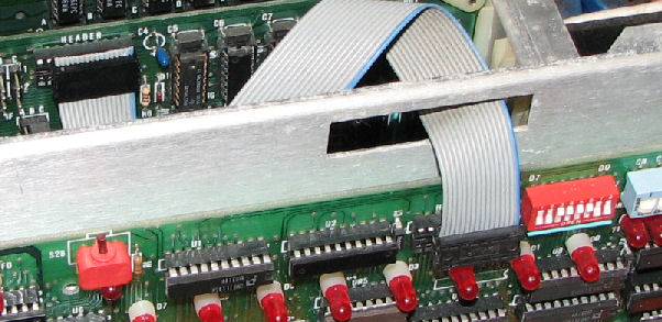
There are many switches on the top edge of the front panel board. These set up wait states, breakpoint features (halt on address), continuous operation of basic front panel functions, and a DIP switch to set what instruction the front panel "jams" into the CPU, through the front-panel to CPU cable. This cable connects the front panel directly to the CPU's data lines, bypassing the bus. Most front panels work by jamming a "jump" instruction (C3 hex for 8080 and Z80) followed by the address as set on the front-panel switches; then the CPU addresses that location and is held so that location's data is displayed on the front panel.
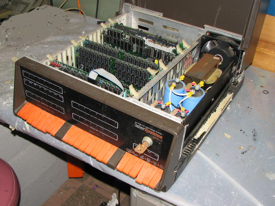
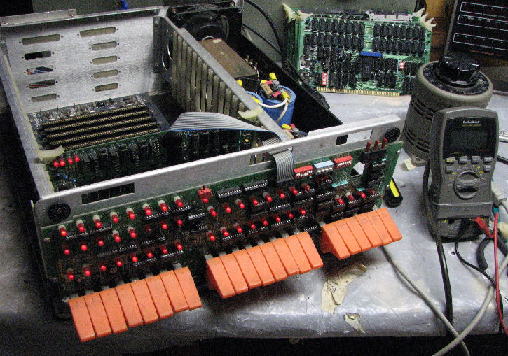
Here's an inside view of Ithaca as originally recieved. Note the rusty key on the front, the dust along the top front edge, paper masking tape on the right side ventillators.
tag the DC cables to motherboard
mold, corrosion: closeup of fuzz on back of 64K card
closeup of fuzz removed from back of 64K card
oxidation on pins of this IC
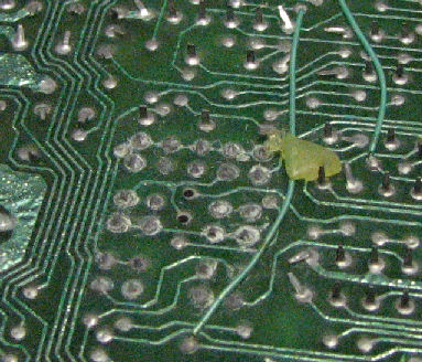
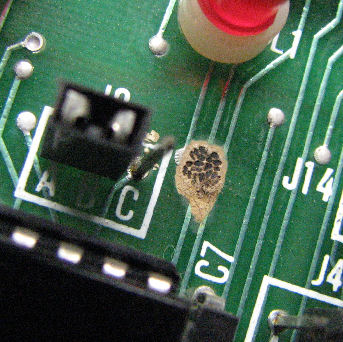
blob of goop on f/p circuit board
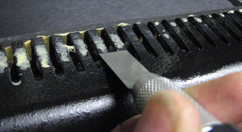
scraping masking tape off edge of cabinet
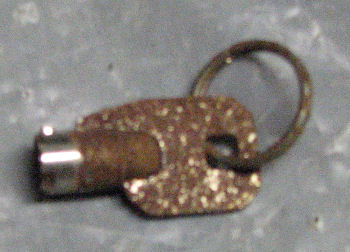
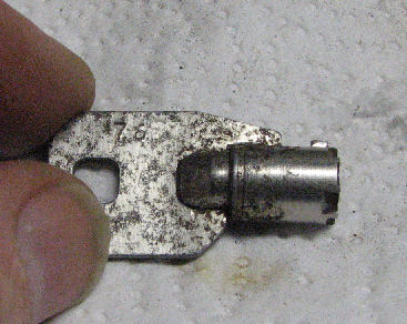
A number of screws had outright rust but these seem to be just cosmetic issues. here's the power switch key before cleaning; and the power switch key after cleaning. On the motherboard, here's rusty bolts on the screws of the voltage regulators of m/b. I used a paint brush to remove any loose rust from these and other locations. (Removing the screws meant removing the motherboard, I preferred not to do that.)
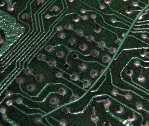
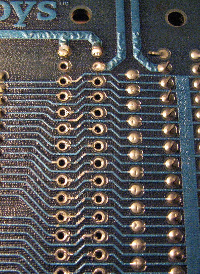
soldering issues: I examined the front panel board and noted many holes along the edge connector were not filled with solder. So I resoldered thsoe front panel through-holes because sometimes the copper in them will corrode or crack and become intermittant.
results: Here's how things look with the front panel and case cleaned up. This is the cleaned Ithaca DPS-1 from the front.
I set up an autotransformer (circular device behind voltmeter) to power up the power supply and then the cards, for a number of reasons. First, it helps to bring up power from zero slowly, to protect the very large power supply capacitors from shorting. Second, the tantalum electrolytic caps on the boards have a habit of shorting and igniting. Third, when S-100 supplies are run under light loads, they tend to be above their nominal 8 volts and 18 volts. (I found with CPU and front panel only, they were about 10V and 20V, so I ran at about 80% AC line voltage.) There were no incidents of blown capacitors with any of the cards tested.
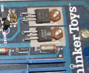
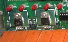
As I raised the AC voltage, I found the Q2 voltage regulator on the right was too hot. But checking the schematic and using the voltmeter to trace the +5 voltage from it (slightly different from the voltage of the other regulator), I saw that it provided current to all the LED's. So it was appropriate for it to run hotter. But I added a small heatsink to the IC; there was space to do so both on the board and behind the front cover.
My digital camera which took all these photos, was very useful for close examinations of the boards, using its "macro" capability. Here's a closeup of a cap on the 64K card, taken so I could read and confirm the component value.
The front panel's address bit display would vary as I flexed the front panel board. I checked the edge connector on the f/p board and cleaned it further with a very soft eraser. But I also examined the edge connector closely, and found copper oxide on S-100 motherboard connector to the f/p. I used a Q-tip in alcohol to clean the connector and remove this material.
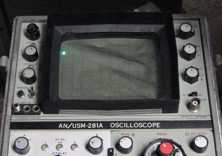
tracing digital signals HP oscilloscope, waiting for trigger
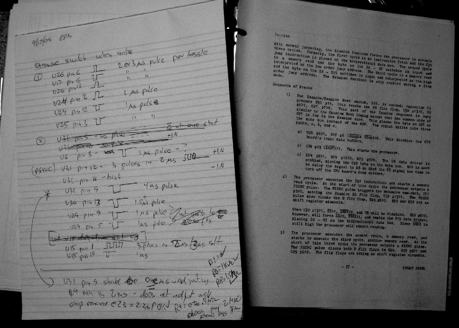
notes on verifying front panel digital activity
I followed the digital signal descriptions in the f/p manual for the "examine" operation. THe local logic seemed correct. I also checked for continuity (ohms) between the DIP switch pin for D0 and the corresponding DIP socket position on the CPU board for D0. As the manual says, both 16-pin cables are "right justified" and sit in the rightmost side of the 20-pin socket. I had to reverse the cable at the CPU from its location as recieved.
cabling and jammed instruction to CPU CPU card with cable in wrong position, as recieved.
front panel and CPU cabled correctly, switches in "C3" position
The final problem with resolving proper front panel activity was due to the DIP switch which jams "C3" jump instruction. This switch was just dirty, data bit 7 did not engage when closed. So "C3" was not actually sent to the CPU, until I forced the switch closed.
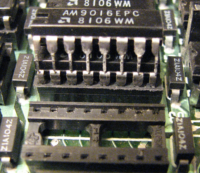
Here's the Ithaca in progress, as I test the 64K memory and ROM on the floppy controller card. I had an odd issue with RAM memory; for any address with the lowest two bits as "1", such as XXX3, XXX7, etc., bit 5 of memory was always a "1". I solved this by deduction. First, I isolated the specific RAM chip on the board by determining which of four RAM banks was active (bank 2) and which chip in that bank was bit 5 (chip "C"). Then I simply swapped that chip with another RAM chip, chip "B"; and observed if the problem moved to that bit - and it did! So I replaced the 9016 16K DRAM with one from some other S-100 card. This solved the problem.
Some "problems" are not problems. When testing the floppy controller, I put it on an "extender" card. This is a card with straight traces from card edge, to a card connector on top, to extend the bus above the chassis, to provide physical access to that card's chips and jumpers. In doing so, I was not able to access the ROM on the floppy controller board. Consulting the manual, and looking at jumpers, I saw that the ROM was accessed at location 0000, bank 0, after reset (a typical configuration). This access can be removed by an I/O instruction to the board; access requires a few bus lines to be active or inactive. I was not able to access the ROM, but experience suggested to me that I try the board without the extender. Doing that, the ROM was accessable. (ROM reveals itself as memory which cannot be modified.) Either the edge connector was intermittant, or as is often the case, the extender card creates distortion and crosstalk sufficient to confuse the card extended.
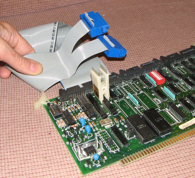
The floppy drive connector for 8-inch diskettes is an ordinary 50 -pin flatcable connector on the board. Oddly enough, the connector has TWO, not one "slots" for a corresponding "bump" or key on the flat cable. Normally it's one bump; I had to shave the connector on a 50-pin cable to accomodate the controller's socket. Of course it's important to identify where pin 1 is, that is where pin 1 of the cable is connected. On cables, that's marked by a colored line on the edge of the cable.
The VIO card has two UARTS for serial connections, either current loop or RS-232; and two 8-bit parallel ports. This version of the card has no interrupt controller chips. I made these determinations after examining the card, as my notes show. In my notes, I trace where the 50-pin flatcable connector is connected to the two serial ports. It's cleverly configured so that Ithaca could make a simple cable using a 50-pin flatcable and two DB-25 connectors to it. I was able to make such a cable, as shown here. It's not a difficult matter, to disassemble some old flat cables for the DB-25's, and reassemble them onto an old 50-pin (formerly SCSI-1) cable. Like the floppy controller, the VIO board's 50-pin connector had two "keys" so I had to shave the single "key" on the cable I made.
At this point, I've got a system in some kind of condition for boot-up tests. The floppy controller's ROM appears at location 0000H, I have a serial cable for a serial terminal, and a floppy drive cable. I set up a pair of 8-inch half-height floppy drives in a Heath cabinet, which I tested on a Z-100 Heath system. With a terminal in place, I powered up everything and stuck a blank diskette in the drive, and started from location 0000.
The results were: sometimes the drive 0 would be enabled (light comes on) and a head load would occur (you can hear the head solenoid); sometimes, no such action. SImple testing, wriggling the floppy controller card, showed some intermittant connection as the data lights for some memory locations would change as the board was flexed.
In the course of testing a few Ithaca disks from another system, one disk's media coating was so brittle (dried out and/or inflexible) that the drive head scraped it off as it rotated around. WHen this occurs on both sides or when one side lacks a coating, you can see the transparency of the mylar "cookie" as a whole track is scraped off. You can hear this occur, although on old drives the diskette hub can squeal in a similar fashion.
At one point I had to check the Heath/Zenith Z-100 system I use to debug and repair 8-inch drives and to test media. Some of the 8-inch floppy drives I set up (YE-Data YE-180's) had some odd re-wiring and jumpering which caused them to load their heads on media even when the drive was not selected. I determined this was a DRIVE problem, not the Z-100's problem. Now, the Z-100 is OK, I have some good drives, and I've selected some Ithaca diskettes from another Ithaca system which have code on the "boot tracks".
In early October 2009, I now have some good drives, some known-ok Ithaca diskettes, and Ithaca cards that appear to be useful.
So, as I work on the FDC's chips, using the Ithaca front panel and my oscilloscope, I can see what the ROM code is doing. I used the front panel to walk through the boot ROM on the FDC and verified I have the correct ASM sources. When I hooked up the floppy drives and tried to read a diskette, it looks like the FDC is stuck just when it's starting to read the diskette data stream. But it's trying to access the drive,a dn that's progress.
The reason I'm now showing my notes and process in detail, is to demonstrate how to debug these S-100 TTL-based systems at the component and logic level. As these are notes in progress and are written both before and after work done, they will be rough notes. Only textbooks provide smooth accounts of real work.
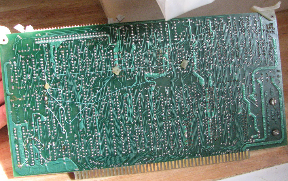
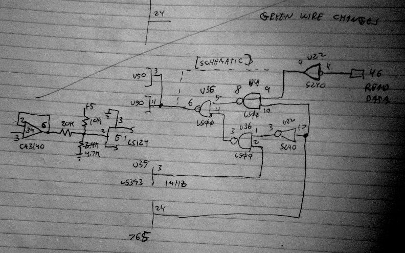
Before I began to probe the FDC board, I noticed that one of the chips was missing! The board is socketed and a 74LS135 chip was absent. Searching through my chip collection, I found a 74135 chip. The schematic says it has limited inputs and outputs - it's part of the read data circuits. Adding that chip, the Ithaca now loads the floppy drive and does some kind of read, times out and unloads the head, and loops in that fashion. I looked closer at the board and saw some rewiring on the back. Patient checking by eye and ohmmeter to trace these wired connections, allowed me to redraw those portions of the schematic to create an update to the schematic for this board.
Then I checked my board inventory, and found another Ithaca FDC with similar wiring. I also found another FDC which was a later revision, with slightly different layout and additional chips! It was not uncommon in the S-100 world of the 1970's, to have many revisions of a floppy disk controller. The technology for floppy read and write was always evolving; it did not stablized until later models of the Western Digital FDC chip set, with similar models developed by Intel and others. It was not until the 1980's that processors were clocking much faster than floppy data bit rates, and these advanced FDC chips with integrated data decoders were available and in use. These were also precursors to chips sets for hard disk drives, which followed a similar and later development path.
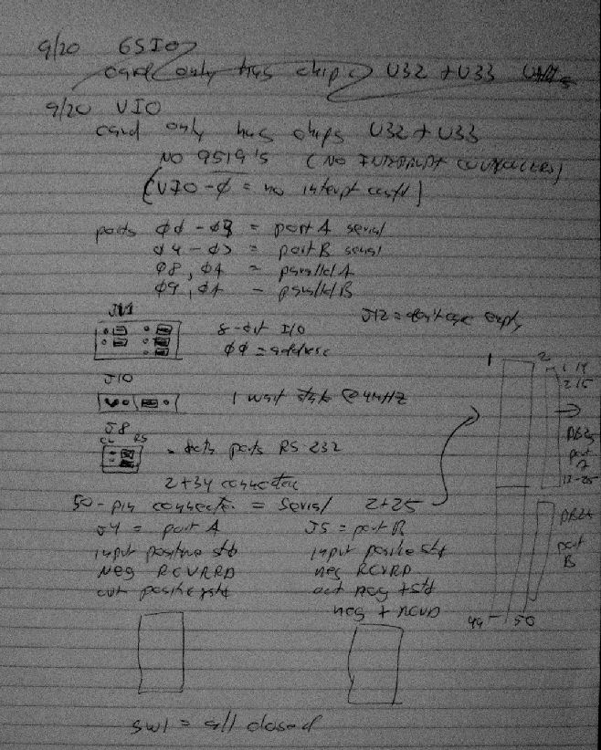
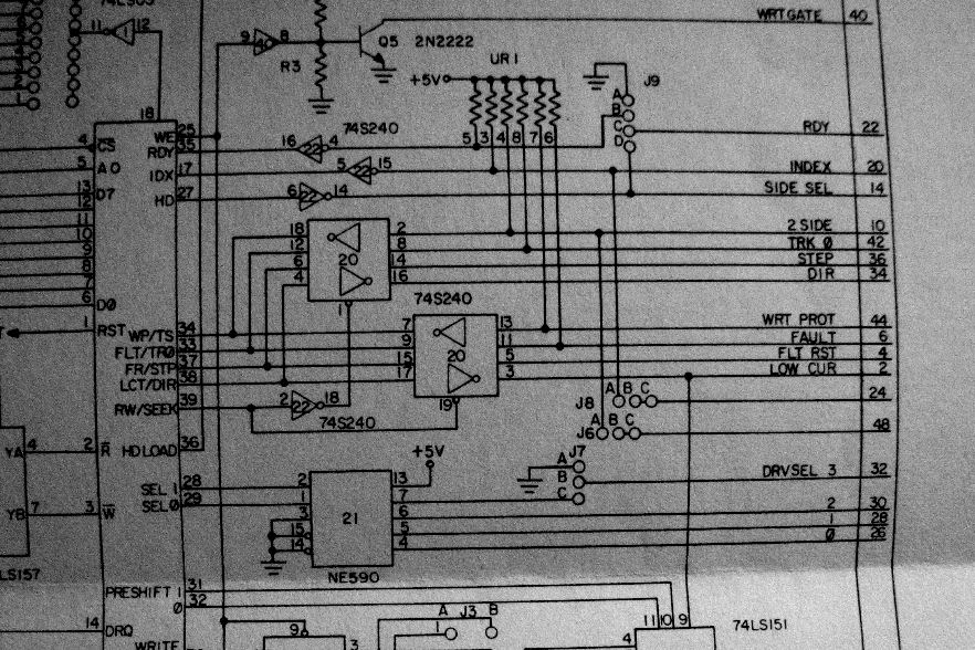
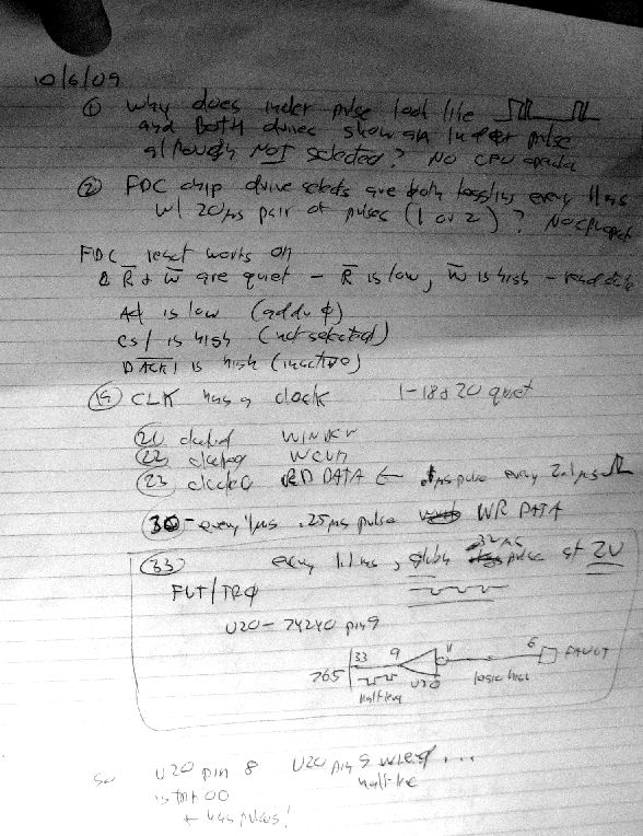
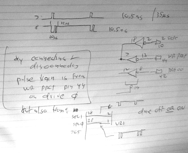
My next step was to use the schematic and my redrawn update, and my oscilloscope, to see what was going on at the logic level around the FDC and floppy drive interface. First, I saw strange extra pulses around the "index" line when the disk was loaded in the drive; but the pulses remained even AFTER I removed the diskette! My rough notes as I traced the issue record that So, something is causing the FDC chip to produce these pulses which the drive returns through "index" and other lines.
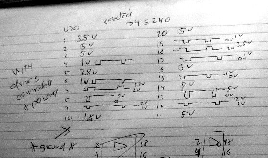
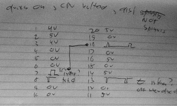
I soon found some odd activity at a few lines going through chip U20 a 74LS240 buffer. Not only was the chip passing pulses through its buffers, the logic levels were in correct. I was seeing logic signals at 1 volt, 2 volt, 3 volt levels - not near zero and four volts as TTL logic normally operates. Do my notes show you the "cause"? Pin 10 of the 74LS240 was not grounded - it was at 1.4 volts! That skewed all the voltage levels in the rest of the chip.
With the chip removed, examined and reseated, the odd logic levels went away, but not the pulse activity! The pulses were on pins 7 and 8 of U20, the buffer chip. By I found that the floppy drive select lines were being pulsed, and so the drive was returning activity at the pulse rate. Here's my notes on this finding that the FDC chip was "driving" these pulses, for some reason. Other lines of the FDC chip have activity as well. Of course the clock line, but there's also a pulse stream on the RD_DATA (read data) lines, Again, some of this is recorded in my notes.
So, at my next session, I'll look over my notes and the schematic, and carefully note the activity around the FDC chip with my oscilloscope. I'll try to track down the source of these inappropriate pulses, at microsecond widths and millisecond intervals.
One evening, I lost use of the front panel, after simply powering up the system. My first thought was to check the DC power, and sure enough an +18V fuse blew. Each DC line to the motherboard is fused. It was not hard to replace the fuse, but that did not restore the front panel. It would not "examine by address". Took a few hours of schematic and scope time, to run through the logic, without much luck. Then, I looked at the manual's signal-level description of the examine address circuits. Walking down the logic, I found a logic level that was not going high enough. Turns out to be the TTL output of the NAND gate which drives XRDY line, part of what drives the CPU board during front panel cycles of activity. But what would cause that output to not pull high enough? Well, it's put on the bus on pin 3 - the +18V supply is pin 2...see what happened? The +18 faulted over to pin 3, and the excess voltage blew the TTL output pullup transistor on the gate.
But solving the cause is not enough. Turns out, the gate is a National DM8092 *five input dual NAND* chip. There are no standard TTL 5-input NAND chips. As a substitute, I'll have to take two 7420's (single 8-input NAND) to replace it! Or find a source for this odd-duck chip. I'll persue both options.
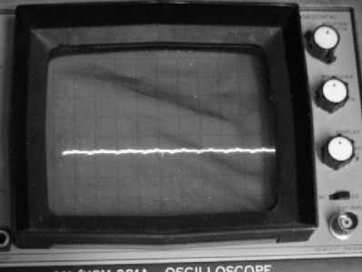
I found a source - David Gesswein did - and it took a month to get the chip. But it was not the problem. I'll explain this out later, but I spent a few days' time looking at more logic levels and seeing a lack of "low" or "highs" that were appropriately low or high enough. I kept seeing problems around bus pins 53 and ???. After replacing or substituing chips, I still saw incorrect logic levels - sitting at 1.4 volts, as seen in this 1 volt/division oscilloscope reading.. Finally, by simple elimination, I pulled ALL the chips on those lines. I still saw 1.4V! Then I realized, this system has a terminated bus.
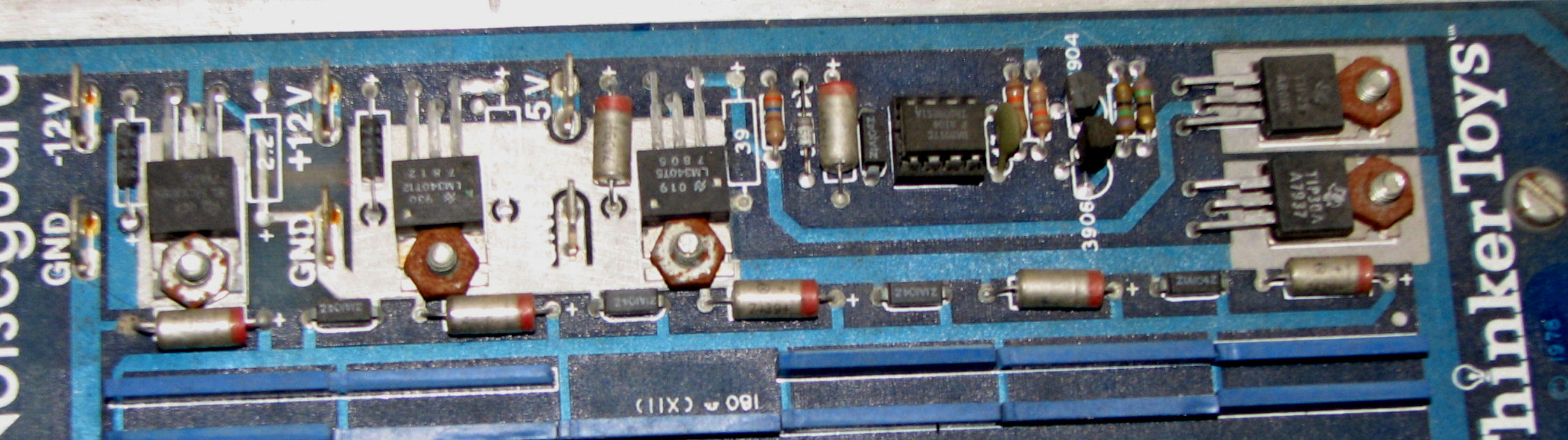
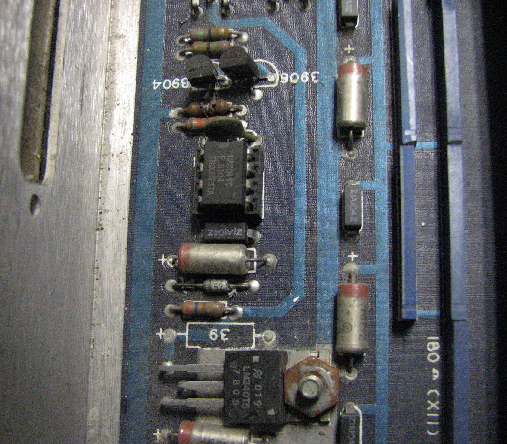
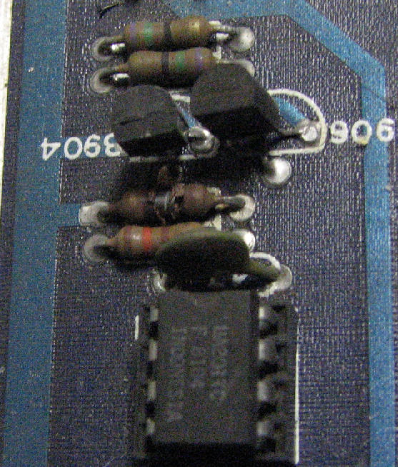
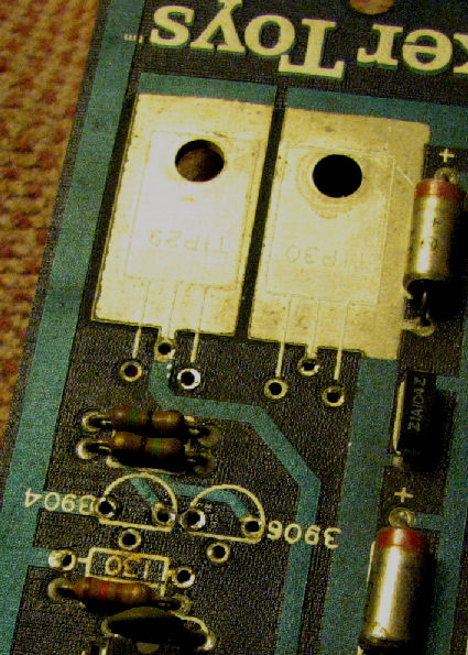
Here's a look at the Wunderbuss terminator circuit, before my recent problems. Rusty nuts but it worked. Here's what I saw when I looked later. Spot any problems? Here's a closer look. See the burned resistor? The same excess current that blew the fuse, burned up this resistor. It read a little low with an ohmmeter. Removing ALL the boards from the bus, the terminated bus lines read the same 1.4 volts. Problem with further diagnosis would be, that I had no schematics for this motherboard.
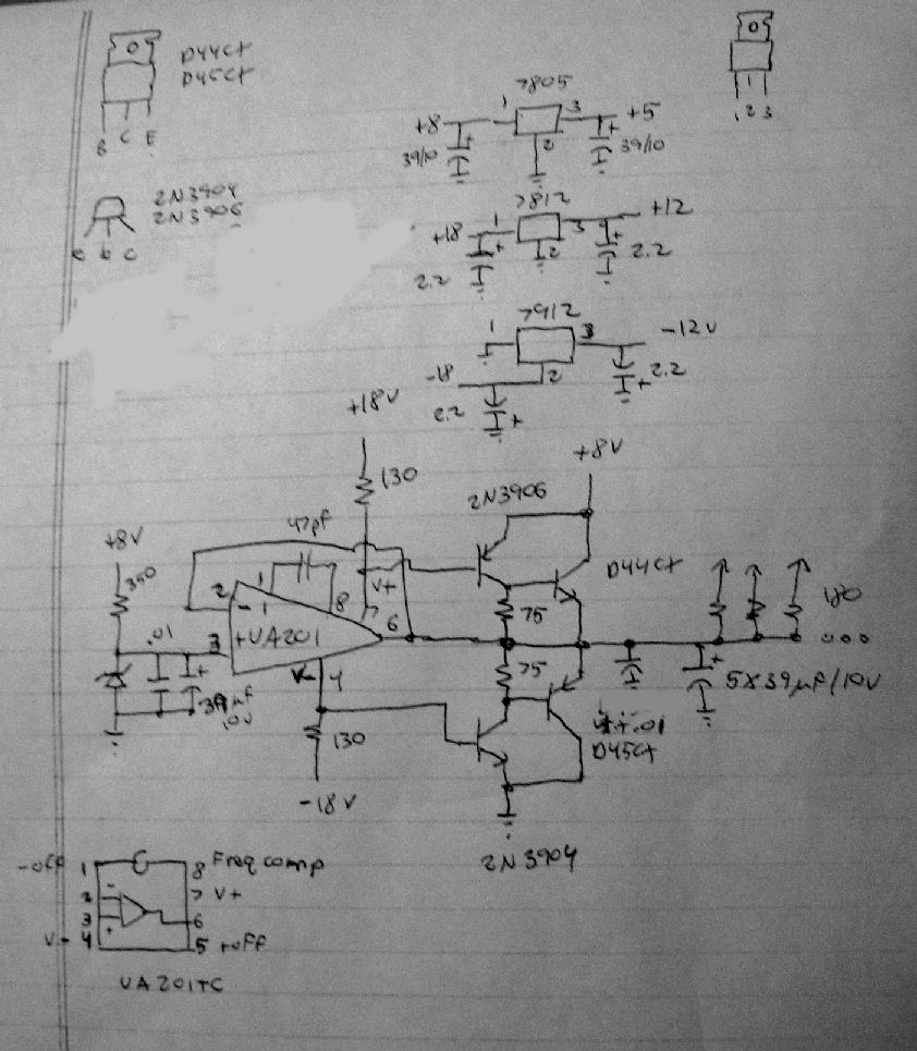
But, it is not a complicated circuit. In fact, it's pretty common in the S-100 world. A voltage source, driving an op amp, which drives a Darlington arranged two-pair set of transistors. I spent another evening, tracing an identical motherboard's circuits, drawing the various connections, and then creating a schematic. The point of the design is to provide a "floating" voltage of about 2.5 volts and an "impedance" of about 180 ohms through series resistances of that value back to the common voltage source (which acts as a current source).
A very similar termination scheme for S-100 is discussed on my Web site at this link. A comparable schematic is this Compupro schematic of their terminator. But my Morrow op amp has -18 and +18 voltage sources, not ground and +5 as used by Compupro's design.
In another evening's worth of hours, I removed this motherboard from the Ithaca chassis, and pulled out each transistor and tested it. Tests were with one digital voltmeter, to check the ohmic resistances of the base-emitter and base-collector junctions AND the "diode" test which reads the forward voltage drop (usually between .55 and .7 volts. Another voltmeter has a transistor test socket on it to read the type (NPN or PNP) the connections (bce, ebc, etc) and to give a "gain" reading or "h sub fe".
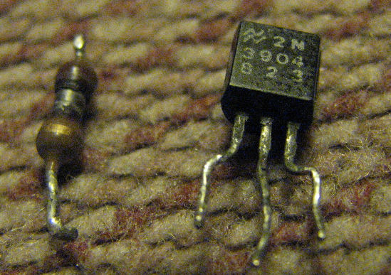
Along with the burned resistor, I found the 2N3094 had a shorted base-collector junction. The base connects through the burned resistor to -18 volts. The other three transistors appeared to be functional.
I know these facts: 1) the +18V fuse blew and 2) the terminator resistor at -18V cooked and 3) the B-C junction is shorted which was connected to that resistor. Looking at my circuit diagram, I can assume the that almost all the 18 volts was across the 130 ohm resistor. V**2/R = power of 2.5 watts - far more than this 1/4 watt resistor was designed for. Even so, it still read 132 ohms before I removed it.
So my guess is that some fault occurred which connected +18V to one of the bus lines. This forced the common current source line too positive. That may have exceeded the base-collector voltage and current limits on the 2N3904, which caused the junction to short, which drew excessive current through both the +18V fuse and the 130 ohm resistor to -18V. The fuse blew before the resistor.
It's a little tough figuring out all the paths, because of the bus terminator. There may be other damage. But my oscilloscope shows some reasonable signal activity on other gates and such; the terminator supply probably kept the other lines from excessive voltages and currents. I'll know more when I restore the bus terminator to normal operation and see what the other bus signals "do".
NOv 8th: I bought some new screws (#6-32 X 3/8") and nuts to replace the rusty ones. (I failed to find nylon screws for the motherboard, they are too close to DC lines.) I carefully resoldered the working power transistors and two new small transistors to the motherboard. I could not find a 130 ohm resistor, but 150+1000 ohms in paralel were equivalent. I reinstalled the motherboard and cautiously applied low AC voltage via my Variac - first to confirm the DC supply lines were on the right lugs. THen I monitored AC and DC voltages to watch the terminator respond, as I brough it up to 100V AC. (With no load, the DC supply runs over 8 volts with that input.) I saw no problems, no hot components; the regulated current source came up to about 2.1 volts where it feeds the resistor network.
Next I added the front panel and monitored the results. The terminator voltage was still at about 2 volts. Then I added the CPU board - and the terminator voltage sagged back to the 1.4 volts I saw earlier. I checked various bus lines but got confusing results, nothing clear. Then, while re-examining the terminator circuits, I shorted two pins on the op-amp chip and saw the terminator voltage change abruptly - and I pulled the plug. Examination of the circuit showed I fried something. Disassembly and removal of the transistors showed the 2N3904 was fried.
I obtained most of a full set of transistors and op amps, and some nylon screws for the motherboard, from my colleague Lee Hart. It was about a week later I recieved them, and several days later I worked on the motherboard again.
Nov 16th:I added two new small transistors and an LM301 op amp, as I did not have a new pair of power transistors and they appeared sound. I considered and even tried to use ground and +8 volts to supply the op amp; connecting 100 ohm resistors in place of the 130 ohm pair to +/-16 volts. All that did, was burn my finger on the small transistor pair, as I raised the DC voltage and monitored the results. So I restored the connections to +/-16 volts, and re-tested the terminator circuit, to see if I damaged the transistors. Fortunately, the circuit was OK and at +7 volts on the +8 supply, the terminator was again running +2.1 volts, with no S-100 cards.
I inserted the front panel board, and raised AC voltage carefully and monitored the transistors for heat, the terminator output voltage, and the LED's on the front panel. At about 6 volts on the +8 supply, the terminator was running 2.1-2.2 volts, the front panel LED's were lit, and +5 was available from those regulators. So far, so good. I expected that when I added the CPU board, it would once again disrupt the terminator voltage level and current supply.
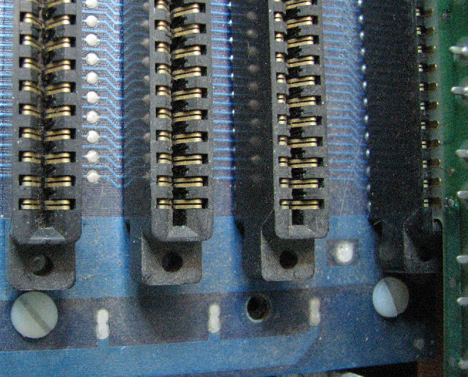
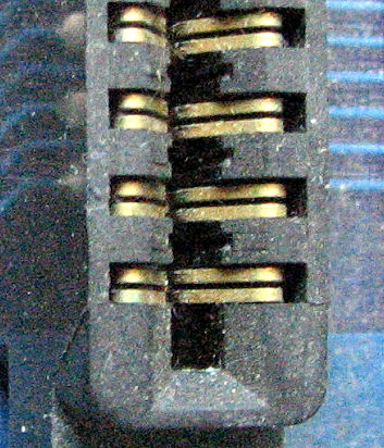
Before I did that, I noticed something about the motherboard connectors. I was still looking for some reason for the -18 volt line (pin 2) to have contacted some other line. Looking closely at the S-100 connectors, I saw that the opposing S-100 pins at +18 and -18V were in close contact. Using my digital camera to take a very close look, some of the S-100 power pins were corroded and had some debris around them. It looks to me, like a bit of movement or further growth of copper oxide could have caused a short of the +18V supply.
My first thought is to add some insulating board in the fingers. My second thought, is to use a lubricant/cleaner I've heard about, in Usenet newsgroup "comp.os.cpm" in Oct 2009. Dow-Corning DC#4 dielectric grease. Quoting Jack Rubin: "These lubes are designed to lower insertion force and prevent oxidation of contacts (the Nye product I'm using is used on things like elevator contacters to prevent arcing) but also work well in low amperage situations. Look at Dwight's and John's results in the attached reference for the numbers. The contact-to-contact wiping force in a well designed connector and undamaged connector displaces the lubricant on insertion. These products are not designed to provide a conductive path but rather to let the connectors do their job in an uncontaminated environment."
Jack referenced a cctalk (private discussion group) thread on the subject. McMaster-Carr lists DC#4 ( Dow Corning 4 ) as Cat# 1204K12 in single tubes for $13.42 each (Dwight Elvey). "I use DC#4 and it works great. It is often used in high voltage applications and an insulator so I doubt it is conductive in any way. I posted about experiments I've done while at Intel, years ago. It improved gold on gold contacts from 10-15 milliohms to less than 2 milliohms. This all while being non-conductive."
Also discussed was "DeOxit", a Caig product, available at Parts-Express "available in a small bottle with a fine tip applicator", for about $25. here's caig's web page about it. I found a local distributor who offers a 5.5oz spray can for about $17.
the previous owner of this Ithaca commented: "For the RAM chips, have you ever tried Stabilant 22? The stuff works miracles. [Here's a Web link about it.] Stabilant 22 is not really a cleaner-lubricant but a semi-conducting fluid that conducts electricity above a certain PD but insulates at lower voltages. They use it in the space program because it resists vibration. It's a bit pricey but goes a very long way. I'm still using a very small bottle I bought about 20 years ago. Does a great job on flaky flashlights, and actually bridged a crack in the motherboard of my old laptop long enough to get the data off." This note at CAIG Laboratories compares DeOxit and Stabilant-22. A Web search on Stabilent 22 reveals more discussion, the gist of which is "DeOxit is cheaper and works well enough."
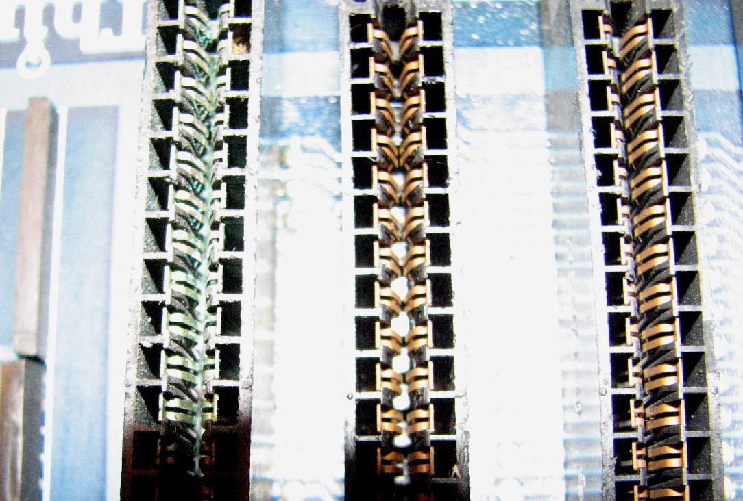
I have another Wunderbuss motherboard, with worst rust conditions, I'm using as a reference. One connector on that board has very rusted pins - copper oxide on and around the connector. Out of curiousity, I wondered if I could actually remove the connector without damage to the circuit board. Two hour's work, and here's some photos:
photo 1, connector and adjacent connector
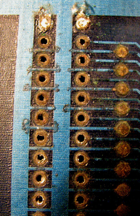
photo 2, PC board under the connector - rusted but lands intact
photo 3, PC board other side - removed without breaking lands
photo 4, under the connector - no through-holes attached to pins
...so it was removed successfully! The connector is shot of course, but the circuit board might become restored.
By Nov 20th I came up with an interrum fix for S-100 connector cross-connecting from corrosion. I simply put a cardboard insert strip in connectors not in use. This keeps them out of each other's way. Meanwhile, I carefully powered up the motherboard and monitored the heat and voltage at the terminator common. It "held" to abut 2.0 to 2.2 volts once the 8 V DC voltage was up to several volts. Then, I added the front panel, and then the CPU. The terminator held true! I'm now back to square one from several weeks ago.
After the route of fixing the motherboard, I still had to determine WHY this Ithaca was not examining addresses correctly. I found myself looking with the 'scope at the process of "examine address", the same chips I looked at before. Logic levels looked slightly better this time. Then I found myself looking at the DIP switch, through which the "jam instruction" circuit worked. The front panel jams an instruction into the Z80 on the data lines (at the proper time) followed by data from the toggle switches on the front panel. The switch determines which high or low - the instruction byte - is used. "JMP" or "C3" for examine.
To my surprise, there are two or three 500ns pulses going through the switch! AND, I found that one bit (D7) was intermittant!. As I had noted before, the DIP switch was dirty and worn. I thought I simply jammed it on enough, but with the oscilloscope to test it "live" I found it did not hold its settings! Now I had no choice, I HAD to remove it, risking damage to the PC board. But since I removed a 100 pin connector, I had some confidence. With a few hour's effort, the switch was off. I put a socket on and an new DIP switch. The fix worked! The panel performed OK.
Nov 19: I added the 64K memory card, and it worked OK. then I added the floppy controller, with its ROM, and I could read the ROM OK. Then I added the VIO card with serial ports, and a terminal. (This is back to where it was before I lost operation several weeks ago.) I ran from the ROM, saw that it was marching through memory (looking for non-RAM) but generally it just kept racing through memory, not waiting at the floppy controller. Again, that was much like before.
I decided to toggle in a read/write to serial port program, from the docs, into 8000H well above the ROM. I hand assembled the code and toggled in the hex bytes. Checked them, corrected a few bits, checked them, corrected a few bits, checked THEM....hey, I keep losing bit D5? Am I not able to toggle bits after 35 years and my first IMSAI??? A few rounds of this and I decided - flaky memory. I checked the docs for where D5 at 8000H must be. Pulled the chip (16K X 1 DRAM) and powered up again to see the results. Hmmm...every other byte had a stuck D5. Must be interleaved memory....
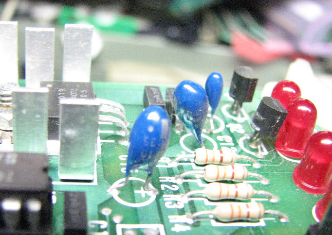
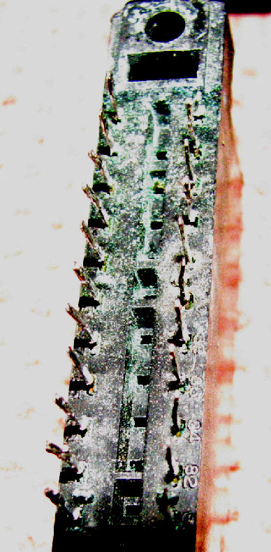
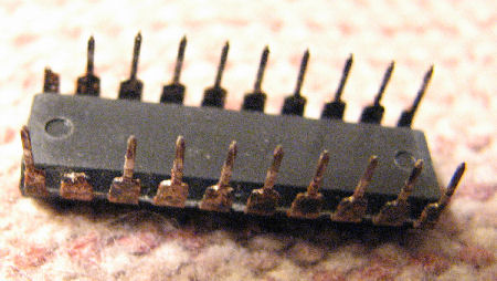
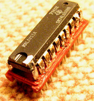
Nov 21: Well, yadda yadda yadda, my chips were rusty. Several of them. Some are corroded, a light white rust. Some are rusty red or black, brittle pins - some kind of copper/silver corrosion, Here's some photos:
rusty chip #1
rusty chip #2
rusty chip #3
rusty chip #4
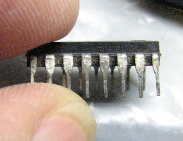
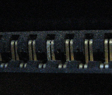
The worst chip was a 74LS688, take a look. The pins are actually RUSTING OFF. It's an odd chip, so I decided to "fix" it by soldering it into a header.
Nov 22: I installed the RAM board, and it failed outright. All bits high, no writes from the front panel changed them.
But this Ithaca came with TWO 64K cards, at adjacent memory blocks. I swapped the block switch settings, put in the other board. Initially it was at least functional. Checking it by entering that IO program again, I again found a bit - bit 2 - was flaky. The same problem on TWO DRAM boards suggests the problem is elsewhere.
But just to check, I examined the second DRAM card, and flexed the board to reseat some of the chips. Result: this board failed like the other one. So I pulled the schematics and looked at the board select logic. I traced the upper address bits A13, A14, A15 - they came through the gates but the last gate was not active when it needed to select the board's RAM. That gate required an active (high) signal from...the A16-A23 bank address logic which compared a bank DIP switch to those address lines. That "logic" is: the 74LS688! (schematic identifies it as a 74LS2521; a TI databook says it's also a 74LS521.) Sure enough, one of the lines from that DIP switch to that chip was not low (.5 volts) but intermediate (1 volt). Pulling the chip, one of two broken pins was the line in question!
Changing a jumper to disable board bank addressing, restored front-panel access to the DRAM board. It allowed me to enter values into RAM and see RAM data (not just 0FFH at every location). So, I need to replace those chips on BOTH boards. I left it at that, for that evening. Later, I found this is a $2 part, if you can find one to buy.
Nov 24: Working with the 64K card, I started to enter portions of that serial read/write program, which failed previous. Well, they failed again. This time, it was bit 1, at ODD byte locations (8001, 8003). When I entered binary 10 at location 8003, it SET bit 1 at location 8001 - and vice versa. Same for entering binary 00 at location 8001/3, it cleared bit 1 at the other location. Now, the card is set up for even/odd addressing, so all the odd bytes are in one set of 8 DRAMS, the evens at the other set of 8 DRAMS. Pulling one DRAM chip confirms this, one ODD or EVEN byte is left short. So, what can be causing this problem?
I physically reviewed the card, and saw two chips which were particularly rusty: a 74LS90 counter chip, and a 74LS74 dual flip flop. The counter chip had a few broken pins when I removed it. I managed to replace both chips with stock in hand (a 7490 in one case, a 74LS74 for the other). These did not change the odd-byte error.
I reviewed the jumper settings on the DRAM card. The Ithaca docs show specific jumper settings for each kind of Ithaca CPU card, 21 jumper sets, some with multiple jumpers. The settings I found match the settings for the IA-1020 "Z80 II" CPU card. But, these cards were built almost 30 years ago in 1981. The DRAMS may not be able to run at 4MHz with no wait states as set up. It may be, some of the address lines need to be active longer, or some of the chips become "confused". Or, it may be DC voltage settings, maybe running the Ithaca at 100VAC is running 12V or 5V (regulated at the DRAM card) too low. My next step will be to come up with ways I can measure any critical timing, or make changes to timing and be able to note results.
- Herb Johnson
In Feb 2016, I restored another Ithaca Intersystems DPS-1 system to operation. To do so, I used the cards in that system, plus other Ithaca cards I had in stock, plus cards from this 2009 system. I also created a bootable Ithaca CP/M disk, from disks which came with that system. Check the linked Web page for all the details.
Work on this chassis, and work with other Ithaca cards in the chassis, was successful and completed late in March 2016. Rather than fill this Web page with another set of details, please look at my Web page on my 2016 repairs and operation of this front-panel DPS-1 and Ithaca-based CP/M. Most of my board work, was done with the previously-restored DPS-1; look at that Web page to understand further details. - Herb
In June 2012 I was asked about replacement front panel switches, by Kip Yeakel. He obtained a FP PC board but only a few of the correct C&K brand model switches, which are long out of stock from that company. I suggested he find some surplus switches and swap some of the mechanical parts to get the combination he needed. (I have, with effort, disassembled C&K brand switches to replace worn internal contacts, parts taken from a good switch with the wrong mechanical features.) But went I took photos and made observations of the Ithaca's switches - I realized how unique these are.
A15 switch photo, left side with paddle removed but adjacent paddle attached
A15 switch photo, front view no paddle
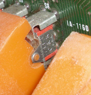
run/stop switch photo, right view from above, with paddle
run/stop switch photo, full right view with paddle, model 7205
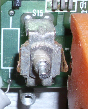
switch descriptions: look at the front panel board view accordingly. In order, left to right are A15 through A0 (Ithaca parts S0-S15), C&K 7113; exam/next, S16, 7205; dep/next, S17, 7205; slow/sing, S18, 7207; data br/addr br, S19, 7203; res/clr, S20, 7205; run/stop, S21, 7205.
The 7113 is SPDT, on-on. The 7205 is DPDT, mom-off-mom. The 7207 is DPDT, on-off-mom. The 7203 is DPDT, on-off-on. Keep in mind, these are late-1970'c C&K part numbers! Also, they are not "complete" numbers, they don't describe all the features of these C&K brand switches.
SPDT and DPDT, look 'em up. On-on means the switch holds two positions, either up or down; on-off-on means the switch holds in all THREE positions. mom-off-mom means up or down is momentary, the switch holds at center; on-off-mom means only DOWN is momentary. Note the physical body and hardware is the same on these, other than the SPDT is thinner than the DPDT.
As I noted above, I was contacted by Kip Yeakel, for help with his rebuilding of an Ithaca Intersystems front panel from a PC board and limited front-panel switches. He identified the modern C&K switch part descriptions for replacements (less the Ithaca paddles), as follows below. details of our discussion and his work, and some commentary from me, is on this linked Web page.
16.         7101J3V6BE2.    Address/Data
2.          7105J3V6BE2.    Ex/Ex next, Dep/Dep next
1.          7207J3V6BE2.    Single step/Slow single step
1.          7203J3V6BE2.    Breakpoint toggle
2.          7205J3V6BE2.    Run/Stop, Reset/Ext clear
Notes on the part numbers:
The first 4 digits describe the switch function and number of poles.
The J3 picks the handle type but the only ones with the proper width are J3 or J10.
The V6 picks the V bracket that supports the switch by soldering to the PCB only V6 or V61
 have the correct size and mounting pin spacing. V61 is a snap fit [with bent mounting pins].
The last 3 letter/number combo picks the contact metal, the sealing material, and the actuator color.
BE2 = gold,epoxy,black. I don't usually care which last 3 I get. - Kip Yeakel
Also note, the C&K address switches part 7101, should be installed so that their paddles can line up (if possible) with the CENTER positions of the other switches. They are not "symmetrical", so it matters which "way" you install them.
Going back to my Ithaca switch descriptions: the original switches are numbered as follows. The 7113 is SPDT, on-on. The 7205 is DPDT, mom-off-mom. The 7207 is DPDT, on-off-mom. The 7203 is DPDT, on-off-on. The MIDDLE position of the 7205, 7207, 7203; is the same as the UPPER position on the 7101. The 7203, 7205, and 7207 switches are symmetrical, in that their center position is in the "middle". But the 7113 is NOT symmetrical, it could be mounted either "middle" and down, or "middle" and up. So.....if you can't get 7113, you substitute 7101 and (probably?) lose the "lineup". Kim noticed this and called it to my attention.
In addition, he and I discussed how to disassemble and reassemble the C&K switch mechanisms. See the details of our discussion on the linked Web page. - Herb
In the winter of 2013, I was encouraged by John King to try to develop a CP/M bootable disk. He kindly sent me some disks he had. I spent the winter examining them on another system, a Heath/Zenith Z-110 S-100 system with 8-inch and
5.25 inch floppy drives and of course CP/M. I reconstructed likely candidate 8-inch
SSSD disks. In the spring and summer, a number of people contacted me to request these disks. By June 2013, I released a few.
THis linked Web page discusses the released re-constructed Ithaca Intersystem disks and also provides the files as a ZIP file. The boot tracks are also included as binary files. in principle, someone could recreate an 8 inch SSSD CP/M disk from those binaries and of course the files. Read the page for more information.
However, the disks I created may not have worked. Check my work
on restoring a DPS-1 system in Feb-Mar 2016 for the Ithaca DPS-1 disks I produced,
and a disk from Kipp, which successfully booted on my currently-working DPS-1 systems
of Mar-April 2016. - Herb
Copyright © 2016 Herb JohnsonCP/M reconstruction and boot
Contact information:
Herb Johnson
New Jersey, USA
To email @ me, see see my ordering & contact Web page.