![[M/S kit]](todd_working.jpg)
Last updated Aug 20 2010. Edited by Herb Johnson, (c) Herb Johnson, except for content written by Lee Hart and others. Contact Herb at www.retrotechnology.com, an email address is on that page..
This page is about P. Todd Decker's construction of Lee Hart's 1802 "Membership Card" Kit (Rev A prototype), including debugging and a single-step circuit. Another construction of a Rev A Membership Card was by Herb Johnson. These are modeled on the 1802 "Cosmac ELF" design of the 1970's.
Todd completed the kit in May 2010. Then he provided Lee Hart and myself with discussion about some design issues Todd uncovered. These were resolved during July 2010: discussion is below. Todd produced a demonstration video on YouTube in July, titled "COSMAC 1802 Membership Card Checkout" by ptdecker. Photos appear on FLickr titled "1802 Membership Card" by ptdecker. Also, Todd also has a Facebook page as ptdecker. - Herb Johnson
Lee Hart and I have been friends and colleagues since the 1980's. Since the 21st century, he's become known for at least two things: electric cars, and work with the low-low-power COSMAC CMOS microprocessor from RCA, the 1802. Go to my Lee Hart Web page to look at some of those activities.
In 2005-06 Lee Hart, in discussion with some of his 1802 colleagues from Dave Ruske's Web site Cosmac Elf, came up with a small card design for the one-time RCA Cosmac 1802 processor which he calls the "membership card". It's built to about the size of an Altoids can, and based on the early "Cosmac ELF" design of the 1970's. In April 2006 he had a prototype for the two stacked circuit boards needed; he completed the PC board layout by the fall of 2006.
But the design languished until 2009, when Lee was encouraged to pick it up again. He produced a few boards and built a prototype, revived his old FORTH for the 1802 called "8th", and discussed his work again with me and in the Cosmacelf Yahoo! group. Several Rev A prototypes were made in 2010, and a Rev B kit was announced in Aug 2010.
The Membership Card home page shows the current status of the Membership Card and kits. It has links to other documents, software, 1802 and Elf Web sites, and so forth. Another Web page discusses the development of the "Membership Card" history, development. For example, there's links to a Web page of 1802 software, such as Lee Hart's "8th" FORTH-like language, his IDIOT monitor, and more. - Herb Johnson
The prototype Membership card was announced early in 2010, and distributed to several people. Check the Development page for Membership Card history, which goes back several years. This prototype is retrospectively called "Rev A" as of Aug 2010. The content below is from email discussions from P. Todd Decker, with his permission. - Herb
April 26 2010: Started stuffing the two boards and they look great! I took a little different tact than Herb in that I plan to cut rectangular holes in the Altoid can and let the switches ride a little higher. It probably isn't as "clean" as Herb's approach, but I think it will work and it avoided having to put little pins into a female RS232 jack that I didn't happen to have a spare of. I found if stuck the leads of the LEDs through a strip of static discharge foam, I was able to hold their bases at the exact height of the flange of the RS232 jack. I plan to do the can this weekend and I'll send photos.
Somehow either the 74HC257 didn't make it into the kit or I lost it, so I'm ordering one (I have to make an order anyway) from Mouser this weekend. I had a second 62256 from when I built the Elf 2K, so I upgraded the RAM to 32K.
Using ultra-low profile sockets for all the chips worked very well. It gives a slight clearance problem on the inter-board connectors but will work. I found the same clearance issue with the supercap but it's really not an issue. I still marvel at how much functionality you've crammed on these boards without using any SMD. Herb's tips on how to install the pins for the inter-board connectors were invaluable, so his documentation is really helpful. I concur with one of your prior posts that some of the holes are a bit larger than they need to be, but I got all to work.
I do have one concern related to the "in" pushbutton. The board has four holes for the in button. The very top hole is the one that is used as the top lead for all the toggle switches, but for the pushbutton, there is no corresponding lead. There is a mounting clip the top of which would align with the hole, but the clip width was way to big for the hole and I ended up snipping them off. The button itself had three leads from it, one common, one N.C. and one N.O. I mounted it so that common was, of course, to the middle hole and the N.O. lead was to the bottom hole so that when you push the button you make contact between the middle and bottom holes. The top pin goes through a top hole you provided for it, but didn't have a solder pad and was thus left unsoldered. All this looks fine and dandy, but my worry is that fourth very top hole. It seems to have a trace running to it. So, do I need to put a small jumper between the very top hole and the N.C. lead??
To stabilize and strengthen the distance between the two boards at the top, I'm ordering some riser sleeves that are the same height as the white intra-board connectors. Then, I plan to run a screw through the RS232 tabs, spacer between the tab and the top board, through the top board, through the riser sleeves between the top an bottom board, thru the bottom board, then put a nut on the bottom. That should hold everything rigid at the top. I don't know if this is what you intended and I couldn't tell from Herb's pics how he had handled this problem.
(BTW, really nice touch having the hole in the top board for access to the trimmer pot!
Finally, what connector should I get (Mouser or Digikey number would be great!) for the power connector??? I believe Herb had a spare in his junk drawer that worked, but I don't and need to order something. I've never been good at selecting interconnects so I thought advice on this point. I glean from Herb's notes and your schematic that the idea is that power can be disconnected from the LEDs only if so desired.
Thank you again for the wonderful design and your thoughts in advance. - P. Todd
Herb responds: Lee Hart made the front case for me, so it's all his work and expectations. I've yet to completely trim the back of the board to fit the Altoids box. The holes for the IN pushbutton are an issue, I think I noted them in my assembly process. You need to put a jumper across as you noted. I'll see if I need to point that out more strongly in my notes. The riser sleeves at the DB-25 connector are a good idea, I planned to do that myself. As for the power connector, Lee should specify it in some way. I happened to have some old 4.5V "CMOS" motherboard batteries with a useful connector, which I keyed as per my notes and photos. - Herb Johnson
Cool on the pushbutton! I'm glad I asked. I guess I did miss them in the instructions, I'll have to go back and re-read. If I figure out a connector part number for the power connector before Lee chimes in, I'll post it back. I'm excited about 'powering up' but just need that one more chip. It will probably be the weekend or so before i get everything finalized. - P. Todd
May 12th 2010: The membership card seems to work (3 AAs for power). I successfully ran Tom Pittman's memory sequencer program and I was able to execute a two line program to turn on Q. I wasn't able to get Tom's "slow blinker" program to flash Q nor my own that works on the Elf 2000. I will hook the MC up to my scope and check out the clock speed to try and get it set. I ran a small program that SEQ, REQ, BZ $00, and Q stayed lit but dimmer indicating to me that I am able to cycle it. I learned that all the switches need to be off when viewing a program since they are wired to the LEDs.
Does OUT 4 work to display something on the LEDs? [It's OUT 5 or OUT 7.] I haven't tried that yet but I need to hit the sack for the evening.
I've said it before, but really cool work. Once the fish paper gets here, I should have everything mounted in the can. I'm making a card stock "front panel" hand labeled for now. I'm putting the three AA batteries, a switch, and LED, into a second can with a sub-mini jack to plug into for power. I've crafted a power cord that works for this. Future project will be to switch to NiCads and mount a solar panel on the top of the second can with simple circuit to charge the nicads. Anyway, off to bed . . . P. Todd
Note: I have a Web page with a blinky program from Lee. - Herb.
[Todd told me later that he was talking to Lee about the OUT latch: ] As you guessed, I can't get things I "OUT" to latch. I'll forward Lee's prior note about the timing diagrams associated with the flip-flop that controls the latching. I will be single-stepping the clock to see how or if mine differs from the diagram. The digram he provided is great and probably should go into the docs. - Todd
May 30: Just wanted to give an update on where I'm at with the membership card kit. If I can get down in my lab, I'll make a de-bounced toggle switch and, perhaps, a one-shot then use them to clock the MC at Ray's suggestion to try and see why my MC isn't latching. At the same time, I'm going to go ahead and order a spare (or two) set of flip-flops and latch chips, just in case I have bad ones. I doubt I can get all this completed this week, but should have it going in a week or two. I apologize for the delays and I'm still sort of a tinkerer (read "n00b" []) therefore my hardware debug skills are not awesome but I take it as a personal challenge to figure out what's going wrong.
Lee Hart says: "The Membership decodes OUT5 and OUT7 for the output port [latch]; INP5 and INP7 for the input latch. Depending on which Elf you are looking at, [I/O locations for similar operations] can change." Here's a Web page where Lee describes how OUT works on the Membership card.
June: Lee and Todd are discussing what's going on with Todd's card. Todd constructed his debounced "step circuit" - here's a Web page about it.. - Herb
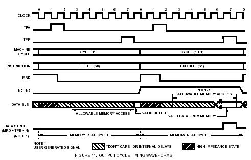
June 17: Todd and Lee determine that Lee's OUT diagram needs corrections (I've corrected this document on this site). That's also figure 11 page 3-15 in this 1802 data sheet PDF, which I've extracted as this JPEG image of the OUT instruction.
(Herb notes: "Todd and Lee use different descriptions for the clock cycle. RCA has their own description: "00" is the first half of the 0 clock cycle, "01" the second half; there's a rising edge in between. "10" is the first half of the 1 clock cycle, "11" the second half, and so on up to cycle 7. Todd says "leading, transition, trailing" for each cycle. Lee says "beginning, rising, end". For example, the RCA data sheets suggest the end of the /MRD pulse is at the "transition" or "rising" part of cycle 1. Lee says "rising", Todd says "leading edge during". Todd's sketch better represents the actual clock.)
![[OUT timing]](todd_step2.jpg)
Todd: Here are my observations [with my timing as observed from the oscilloscope, versus Lee's design sketch]:
* As suspected, my U7 outputs are not latching as they should.
* Taking into account the clock differences, our TPA (U1 pin 34) signals match each other. Both are high during the '1' clock cycle. In my case, TPA goes high during the trailing edge of my '0' cycle clock transition and back low on the trailing edge of my '1' cycle clock transition. Looking at the data sheet, this looks right--both of us are high during '10' and '11'.
* Our TPB--FF CLK (U5 pin 3) do not match. You show yours high during the '6' clock cycle. In my case, it goes high on the leading edge of the clock transition that occurs during cycle '6' and then back low on the leading edge of the clock transition that occurs during cycle '7'. So, my TBP is effectively delayed half of one of your 'cycles' but is the same duration. Looking at the data sheet, it looks like my behavior is correct--my TPB is high during the '61' and '70' timing cycles.
* Our /MRD--FF RST (U5 pin 4) do not match. You show yours high during cycles 7, 0, and 1; then low for cycles 2 through the next 7; then, high again during the next cycle 0. On my membership card, I observed /MRD going high on the trailing edge of the clock during cycle '7' and then back low again on the leading edge of the clock during cycle '1'. Looking at the data sheet, this is the behavior shown occurring during a read cycle--/MRD is high during the '00', '01', and '10' timing cycles but low at all other times.
Lee says: "This agrees with RCA's timing diagram (fig. 112 in MPM-201C "User Manual for the CPD1802 COSMAC Microprocessor"). [Also see this drawing. - Herb] It shows /MRD low during the "fetch" cycle (to read the OUT instruction), and going back high at end of clock cycle '7'. Then /MRD goes low during the "execute" cycle at the rising edge of clock cycle '1'. Finally, /MRD returns high at the end of clock cycle '7'.
* Our N+LOAD--FF D (U5 pin 5) match. We both have it high during cycles 0 through 7. On mine, it goes high on the trailing edge of the clock in the first cycle 7 then it goes low during the trailing edge of the next cycle 7 clock. This matches the data sheet timing for N0:N2 on page 10 of the data sheet.
* Our OUT57--FF Q (U5 pin 1) do not match.... Mine has it going high on the leading edge of the clock transition during cycle 6 and back low on the trailing edge of the cycle 7 clock transition. My behavior looks correct since Q going high matches with the timing of TPB (the FF's clock pin) since N+LOAD (the FF's D pin) is high during that time and it is pulled back low again when /MRD goes high which is tied to the FF's RST pin. [Lee confirms Todd's timing.]
* You should your U7 outputs latching the new data starting during cycle 6. Mine shows the U7 outputs going high on the leading edge of the cycle 6 clock transition (matching OUT57) but then back low again in conjunction with OUT57 on the trailing edge of the clock transition during cycle 7.
*I looked at figure 11 in the data sheet too and everything seems to jive to it as well. [That's also figure 11 page 3-15 in this Intersil 1802 data sheet PDF which I've extracted as this JPEG image of the OUT instruction timing chart. - Herb]
Lee says: "Correct. U7 should pass data to its outputs when TPB goes high, at the rising edge of clock cycle 6. U7 should latch that data when /MRD returns high (resetting the Q output of U5A back low." It sounds like everything works right up to U7, so I think you are right that the latch must be bad."
![[OUT timing]](todd_trace.jpg)
Todd says later: "I swapped out the 373 and, much to my frustration, it still isn't latching. I switched my program to simply OUT5 $FF followed by BR $00 which, in theory, should keep the LEDs lit all the time. However, they continue to just pulse away. I then checked all the input and output pins of the 373 with my logic probe and everyone of them is pulsing. Pin 11, G, is pulsing too. So I hooked up my scope and first probed the output lines and Pin 11--they correspond so that the outputs are going high at exactly the same time as G, but then going back low with it instead of latching. It is acting like a transparent latch that never latches. I then scoped pin 11 and the D0 pin (pin 3). The picture of this trace is linked here. The top trace is pin 11 (G). The bottom trace is D0 (pin 3). The vertical units are 2 volts per division. The horizontal are 20uS per division. You can see when G goes high, a high value is present on the data lines as expected. So, I don't understand why it is not latching."
![[OUT timing]](mship_3gate.jpg)
Herb says: "Lee's description above is consistent with his circuit design. HOWEVER, the problem is that the data should be latched NOT at the end of /MRD (at the beginning of clock 0), but at the earlier, falling edge (or end) of TPB (at the "center" of clock 7). Tood, the latch "latches" on the falling edge of the clock. If that edge is late, when the data lines are unstable, it won't catch the data. Todd's falling edge of G matches the falling edge of D0 - it should be earlier in time.
Check the 1802 data sheets, the timing for stable data is relative to TPB and not /MRD. On my OUT instruction chart, it says "user generated data strobe (/MRD & TPB & N)" which is essentially a gated version of TPB. With Todd clocking it at 0 Hertz, he's got to use the right strobe signal - it's the acid test. Also look at some other 1802 circuits - see what signal they use as an "edge" to time the "latch" of data for OUT operation."
I came up with a circuit to get the timing right, but it takes a 4025 chip, three 3-input NAND gates to do it. I show rough timing for the OUT, IN and DMA IN operations." - Herb
Lee says: "I keep meaning to look into this, but haven't had the time yet. I think [Herb is] right; the circuit needs to be changed. It is complicated by my addition of the MOSFET to switch off the RAM for all but the time TPB is high. I also think that a 74HC374 in place of the '373 should work. But I haven't had time to try it yet." - Lee
(Lee suggests the 74HC374 because it has the same pinout as the '373 but the data is latched on the RISING edge of its clock, not the falling edge. That would catch the data earlier and not "late" in the RAM's READ cycle. My concern is that it may create a "race" condition between the RAM becoming active and the "latch" of its data lines, at the "same" clock time. Look at Todd's "observed" chart of "OUT 57" to see the clock signal timing. - Herb)
(Todd orders the 74HC374 chips which take time to arrive and test...)
Todd, July 10 2010:I received a few 74HC374 chips, swapped one in for U7, powered it up, entered the test program, and it worked. I was then able to successfully run a program that alternated the even and odd LEDs with a delay loop between. I'm assuming that the 74HC374 for U7 is what made this fix. I didn't change anything else. Simply pulled the two boards apart, pulled out U7, replaced it, put the boards back together and powered it up.
I noticed something else. If you go back and look at the video I posted, you'll notice that when in read mode the values of the switches would be displayed on the LEDs at the same time as whatever was in the memory location being inspected. I was having to turn all the switches off to truly see what was in each memory location. [Note: I'd noticed the same thing. - Herb] This also, has been fixed. Now, the value of the switches only latches to the LEDs after pressing the 'input' switch. And, I can step through memory with the switches set to anything and easily inspect what is in each location.
I feel so satisfied! I'm now getting it all into the Altoids tin--putting the fish paper at the bottom and making a paper "front panel". I'll post picks when done (probably monday or tuesday) to the Yahoo group. - P. Todd
Lee says: "Yes, [what you describe is] the way it is supposed to work. Setting the switches should have no effect on the LEDs until after you press the IN button. The LEDs are showing the value read from memory; not the switch settings."
I think the '374 fixes the present problem. The '374 captures the data at the rising edge of TPB (plus the propagation delay of the U5A flip-flop). The memory chip is active long before this, and stays active long after this, so there will be valid data on the data bus.
However, Herb Johnson is also correct that there is a design issue that I want to address. The present design leaves the memory chip active for the entire bus cycle (8 clock cycles). Most modern RAMs draw a high supply current when chip enable (CE) is selected: they aren't true CMOS. So, leaving the RAM selected a long time increases power consumption.
[Later, I came up with this design change] to only pull /CE low when TPB is high. This [enables RAM] only 1/8th of the time, so it cuts RAM power consumption by 8:1. But if I make that change, then I can't use the rising edge of TPB to latch a '374 at U7 -- if I did, then the RAM would need an access time faster than the propagation delay time of 4013 U5A (about 150 nsec). Many RAMs aren't this fast. It would be better to enable the RAM with the rising edge of TPB, and latch the data from it with the falling edge of TPB. I just need to figure out a way to do this (and fit it on the tiny board)." - Lee Hart
late July 2010: Todd has some image and videos of his Membership Card, see links above.
early Aug 2010: Lee Hart designs a "revision B" Membership Card that fixes this data latch problem and also deals with selecting memory. Lee says:
"A RAM data sheet normally says it will disable its output in 50ns from /OE going high. 1802 /MRD going high both disables the RAM (sets /OE high) and resets the 4013 to make the Enable of the '373 go high (latching the data). The 4013 data sheets spec a propagation delay of 70-200nsec. Mine must have been fast enough to pull the 373's enable high before the RAM removed the data from the bus.
"Changing the '373 between C, HC, or LS shouldn't affect this; all of them latch the data essentially immediately when Enable goes low. It's mainly the 4013 delay that's the issue. If there was a 74HC4013, it would have solved the problem by being much faster than 50ns; but there aren't any.
"I changed to the '374 because it latches on the *rising* edge, rather than the trailing edge. The rising edge occurs when TPB goes high (plus the propagation delay of the 4013). This unconditionally works with the existing board, because the RAM is selected well before TPB.
On the new design, I select the RAM on the rising edge of TPB (to reduce power consumption). This means the 4013 must have a propagation delay equal to or greater than the RAM's access time. To guarantee that this is always true, I added a capacitor [to ground] on the Q output of the 4013 [to increase the rise time]. On a sample of one, 82pf was plenty (though I may readjust this later when I have more chips to test)." - Lee Hart
See this Web page for all the Rev B changes. For the latest on the new revision and on the M/S card, refer to the Membership Card home page. - Herb Johnson
This page and edited content is copyright Herb Johnson (c) 2010. Contents written by Lee Hart, are copyright Lee Hart (c) 2010. Copyright of other contents beyond brief quotes, is held by those authors. Contact Herb at www.retrotechnology.com, an email address is available on that page..