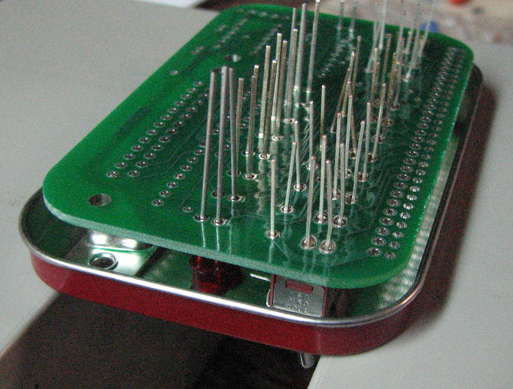
![[kit]](mship_kit1.jpg)
Last updated Aug 20 2010. Edited by Herb Johnson, (c) Herb Johnson, except for content written by Lee Hart and others. Contact Herb at www.retrotechnology.com, an email address is on that page..
Lee Hart and I have been friends and colleagues since the 1980's. Since the 21st century, he's become known for at least two things: electric cars, and work with the low-low-power COSMAC CMOS microprocessor from RCA, the 1802. Go to my Lee Hart Web page to look at some of those activities. This page is about one construction of Lee Hart's 1802 "Membership Card" Kit (Rev A prototype). Another construction of a Rev A Membership Card was by P. Todd Decker. These are modeled on the 1802 "Cosmac ELF" design of the 1970's. Several Rev A prototypes were made in 2010, and a Rev B kit was announced in Aug 2010.
The Membership Card home page shows the current status of the Membership Card and kits. It has links to other documents, software, 1802 and Elf Web sites, and so forth. Another Web page discusses the development of the "Membership Card" history, development. For example, there's links to a Web page of 1802 software, such as Lee Hart's "8th" FORTH-like language, his IDIOT monitor, and more. - Herb Johnson The prototype Membership card was announced early in 2010, and distributed to several people. Check the Development page for Membership Card history, which goes back several years. This prototype is retrospectively called "Rev A" as of Aug 2010. - Herb
ELF Membership board: ELF Front Panel board: The PC connection allows the PC to completely control the front panel; and thus load, examine,
and run programs, and read/write to the I/O ports.
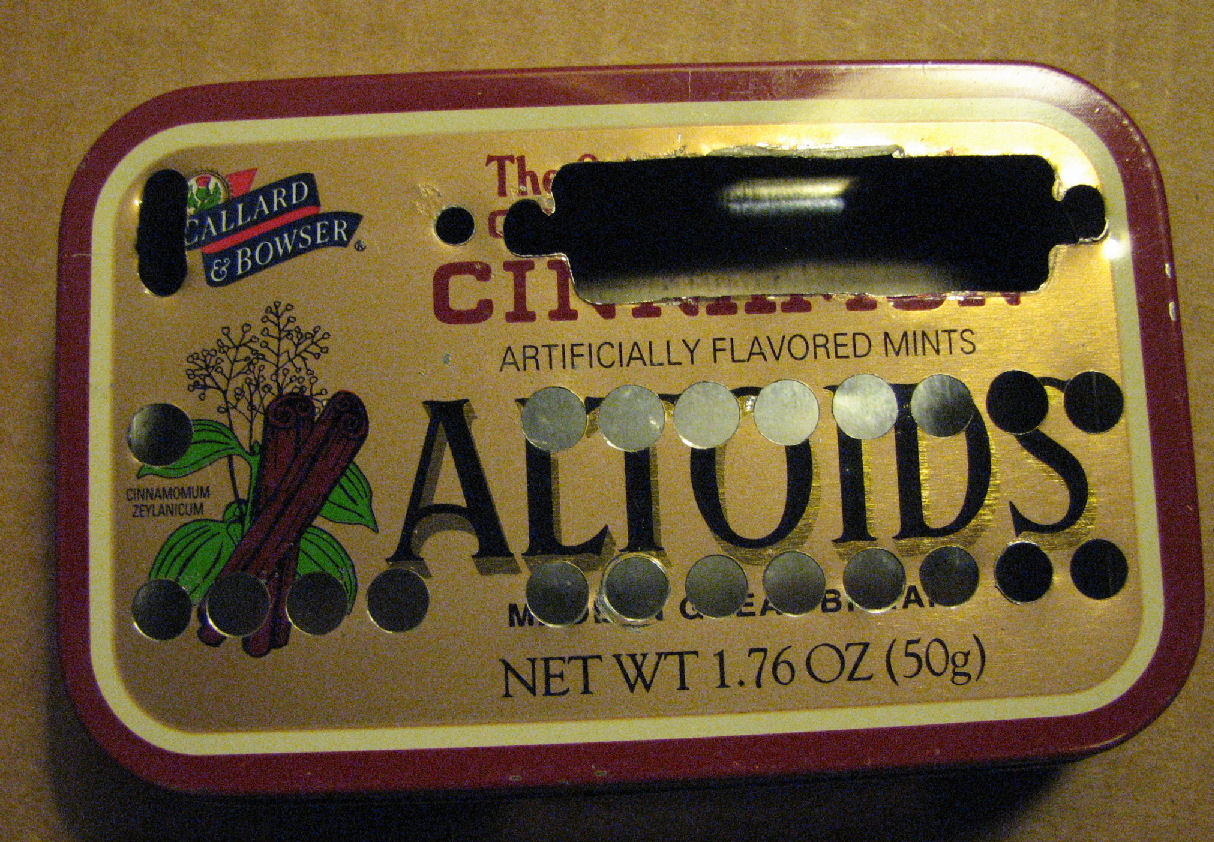
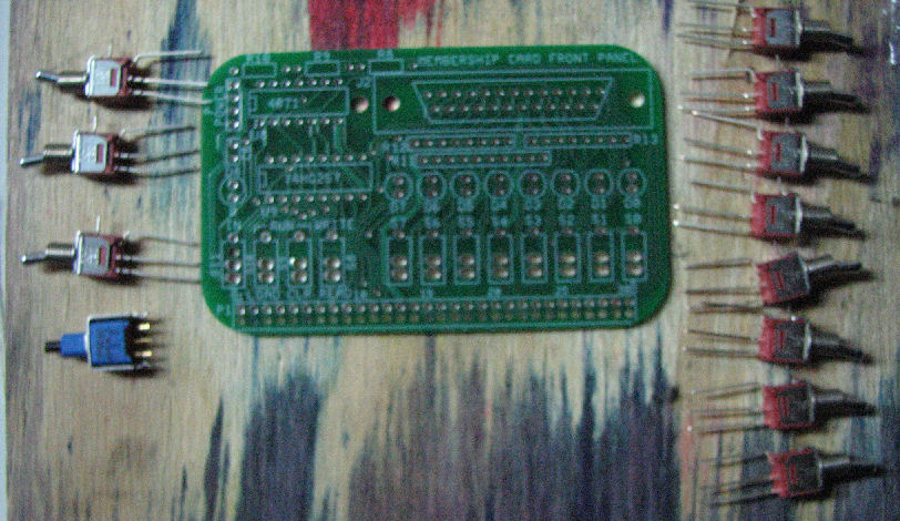
The membership card kit, upon arrival. The instructions are on one-and-a-half pages, as a "work in progress". There are many cautions about how to assemble the boards so they can fit within the Altoids box. That means very low profile sockets for the IC's, and selected components. Some old-school components Lee expected to use, were not available for this kit, so parts had to be adjusted.
On Feb 15th, I began to assemble the front panel card. This assembly is mechanically critical, because the PC board must fit tight against the top lid of the Altoids box, so the CPU board can fit underneath.
Here you can see the inside of the lid, and the array of holes. Here's some of
the components and connectors, excluding the IC's.
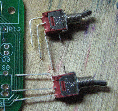
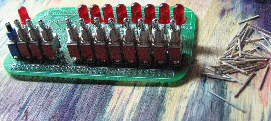
The switches provided were right angle mount. Lee advised how to straighten their leads. Note the three holes for S0 on the board.Here's all the switches, prepared for insertion.
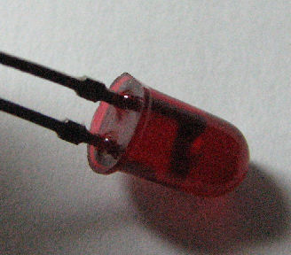
Next the LED's must be inserted. The flat edge of the LED shows the polarity.
The board has a corresponding sketch for each LED's orientation, such as for D0 in this photo.
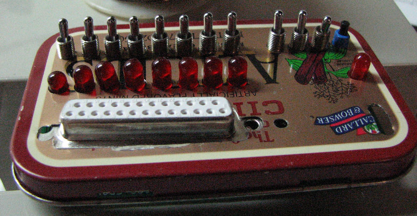
Here's the switches, LED's and the DB-25 as inserted, but not soldered, into the board. The blue push-button switch is loose. Now the lid is lowered onto the switches and LED's, to align them.
The tallest components are the switch bodies. here the lid is down to expose the solder side of the front panel. I use some blocks to support either side of the lid above the table. Note, the DB-25 connector's leads are too short. The LED's must be pushed above the PC board to poke through to the lid ( down in this photo). I decided to only solder one pin per component, not cutting leads, so I could confirm their position and still change it.
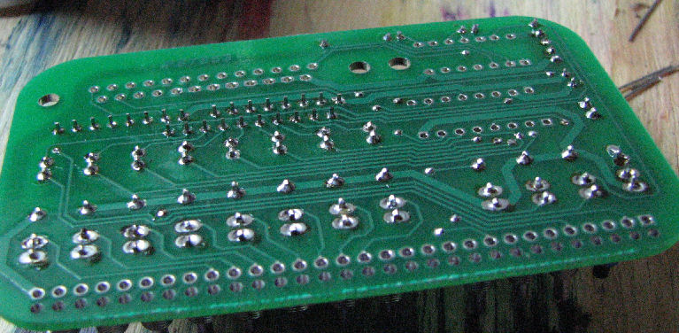
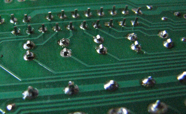
Here's what the "front panel" looked like after initial soldering. Note the LEDs which are too low; I had to resolder them. When I corrected and confirmed the positions were correct, I cut the leads and completed soldering the switches and LED's. Here's the front panel board with switches and LED's in place and leads soldered and cut. See all the solder points on the back? WHich ones are not soldered?. Hard to tell, but here's a closeup of a few "open" holes. Before mounting and soldering other components, I soldered all the "through holes", where there's no leads but a hole to connect traces between front and back.
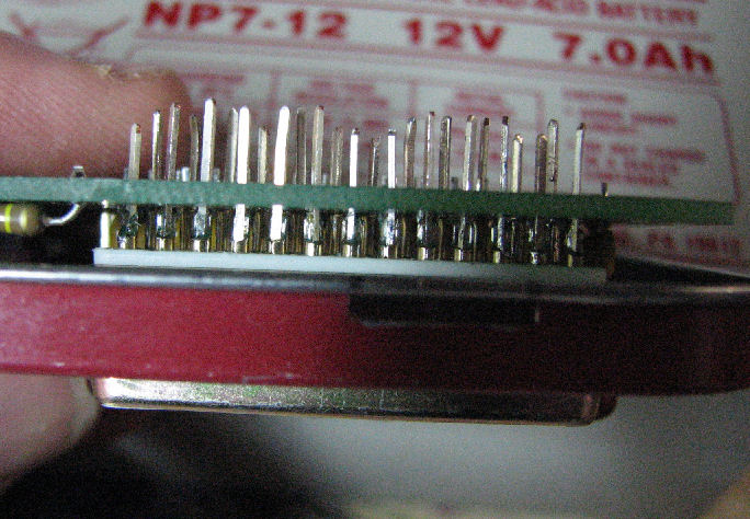
Here's the front panel board with all components in place except the DB-25 connector. I decided I'll use a solder-cup DB-25 and add leads, so it will be tall enough to reach the lid.
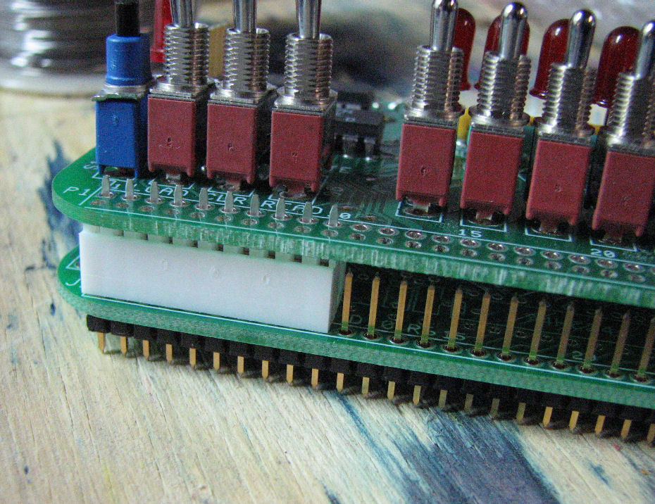
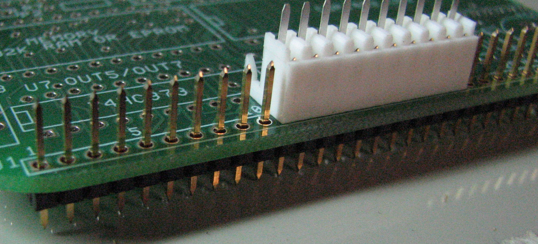
But first I wanted to see how the board-to-board connection would work. Lee provided a header pin
strip for the CPU board, and a white connector for the f/p board. Here's a photo of how the two
ought to "mate". Here's another view, showing how the stacked boards should look. That ended my work for that evening, a few hours after starting to assemble the kit, with a few interruptions.
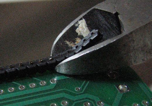
It was tricky, but here's how I used a solder cup DB-25. I took the snipped pieces of lead, put them
in the solder cups. They stood upright, the cups are deep. Then I carefully soldered them while they were vertical, one at a time. Insert, solder, insert, solder. Then I still had to straighten the leads to get them into the circuit board. Rocked the leads into place from one end of the connector to the other. About half an hour's work but it was done. Here's the DB-25 inserted into
the board, before final soldering.
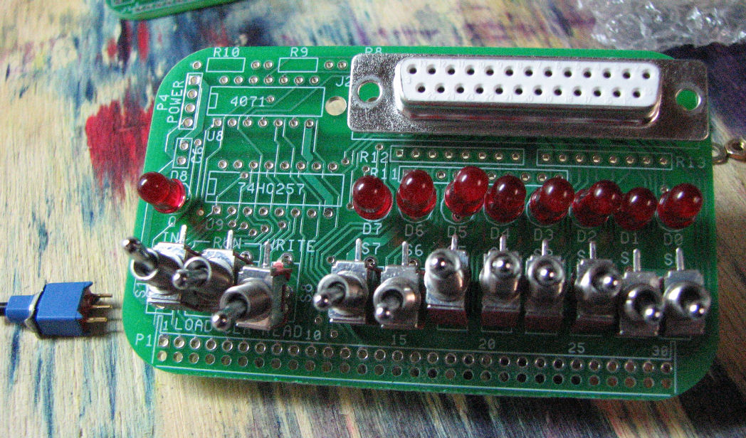
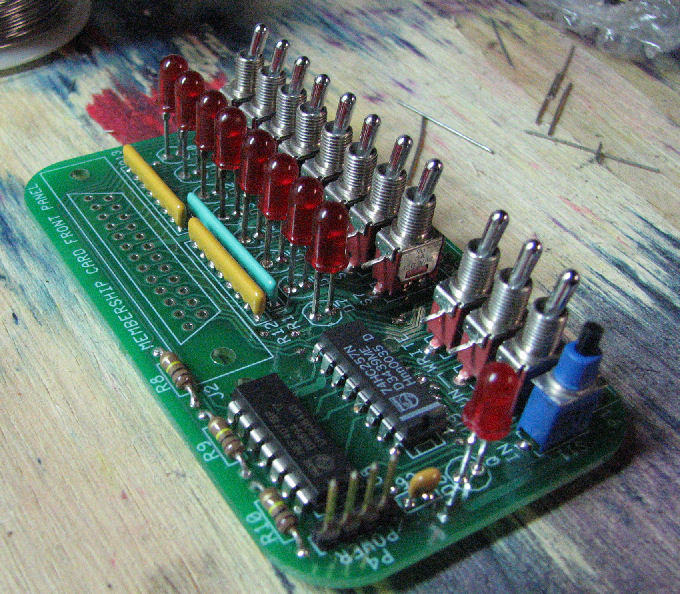
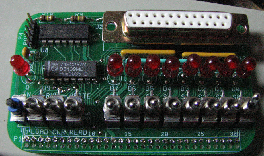
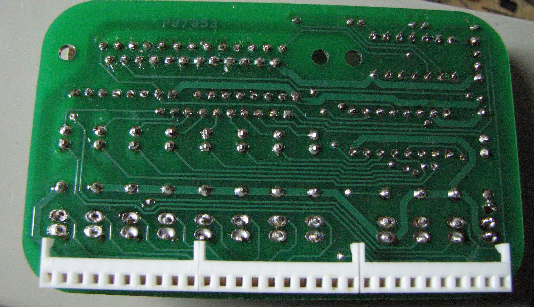
Here's a view of the assembled f/p board.. To see the back of the board, here's the back of the f/p board. (The board cross-connectors were added last, see the CPU assembly information below.)
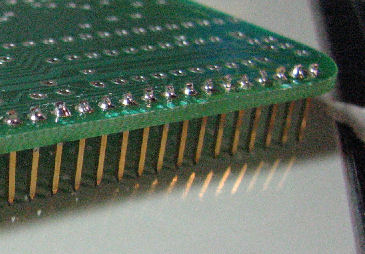
I started on CPU board assembly. Look at photos above for a "dry fit" of the board cross-connectors. To solder the "pin" connectors to the CPU board, I used one of the "sockets" to hold the connector in place. I soldered a few pins at the far ends, then removed the connector and soldered the rest. Then I flipped the CPU board and snipped off the pins "above" the plastic black strip which held them in place. Then I used the snips to lift up the plastic holding the pins, and snipped it off a few pins at a time. Don't use too much force, or you'll pull up the pins! With the plastic removed, I cut what remained of the pins, again. (I had to cut these pins twice, or it would be too hard to remove the black plastic.)
Then I went back to the front panel board, to add the "socket" connectors. In this photo, the CPU board is used to "level" the front panel board, while the sockets are in place. Once the sockets are soldered in, the CPU board can be fitted underneath.
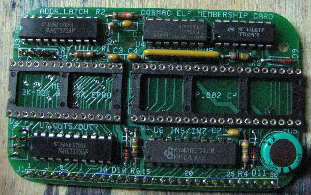
Rev A Membership card, parts and features
Features
Parts List
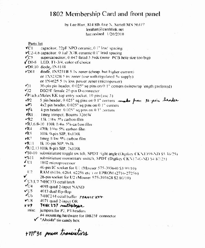
Membership board parts list: [revised 3/22/10]

C1      22pf NPO ceramic capacitor, 0.1" lead spacing
C2-4,6  0.1uF Z5U or X7R ceramic capacitor, 0.1" lead spacing
C5      0.047 farad 5.5v memory backup capacitor, 0.465" dia, 0.2" lead spacing (PC board hole too big)
D0-8    LED, T1-3/4, color of choice
D9,10   signal diode, 1N4148 etc.
D11     zener diode, choice:
	1N5231B 5.1V (cheap but uses higher current)
	or 1N5232B 5.6V (use with regulated 5V supply)
	or 1N4625 5.1V low poer zenor (micropower)
J1      30-pin header, 0.025" square pins on 0.1" centers (wirewrap length preferred)
J2      DB25F female 25-pin D connector, with #4 mounting hardware
J3-6    jumpers, .1" spacing, to short pins in P2 and P3 (configuration for U2)
P1abc   MOlex KK top entry socket, 10 pin, Digikey WM3241-ND (need 3)
P2      5-pin header, 0.025" square pins on 0.1" centers, from 36-pin header
P3      4x2 pin header, 0.025" square pins on 0.1" centers (2 removed)
P4      4 pin header, 0.025" square pins on 0.1" centers
R1      trimpot, Bourns 3266W or eq, 0.25" square, 0.1" lead spacing
R2      15k 5% 1/4w resistor
R3,6    100k 5% 1/4w resistor
R8-10   470k 5% 1/4w resistor <---changed 3/22/10 HRJ see this note
R4      470k 5% 1/4w
R5      100k x 8, 9-pin SIP, one side bussed
R7      1meg 5% 1/4w resistor
R11     1K 10-pin SIP, 9X1K
R12,13  100K 8 pin SIP, 7 X 100K
S0-10   submini toggle switch SPDT right angle (Digikey KCN1059-ND, $5+)
S11     submini momentary switch SPDE (Digikey CKN1740-ND, $4.87)
U1      CMOS CPU, CDP1802, use 40-pin low profile socket (Mouser 575-393640, $4)
U2      2k-32k CMOS RAM (6116, 6264, 62256) or EPROM (27C16-27C256)
        use 28-pin low profile socket (Mouser 575393628, $3)
U3,7    CMOS octal latch, 74HC373
U4      CMOS quad 2-input NAND gate, schmitt trigger, 4093
U5      CMOS dual D flip-flop, 4013
U6      CMOS octal buffer, 74HC244 or 74AHCT244
U8      CMOS 4071 quad 2-input OR
U9      CMOS 74HC257 multiplexer

Front panel board:

C6      0.1uF Z5U or X7R ceramic capacitor, 0.1" lead spacing
D0-D8   LED, T1-3/4 high brightness
J2      DB25F female connector, PC mount
P1      30-pin female top entry socket for J1, Molex KK series
    Molex 22-18-2101 (10-pos; use 3)
P4      4-pin header, 0.025" pins on 0.1" centers
R8-10   100k 5% 1/4w
R11     1k x 9, 10-pin SIP, one side bussed
R12,R13 100k x 7, 8-pin SIP, one side bussed
S1-10   SPDT toggle switch, C&K T101 series
S11     SPDT pushbutton switch
U8      CMOS quad 2-input OR gate, 4071
U9      CMOS quad data selector, 74HC257

Altoids brand, tin candy box
Feb 2010: The kit arrives: photos
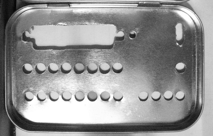
The Altoids case, drilled out.
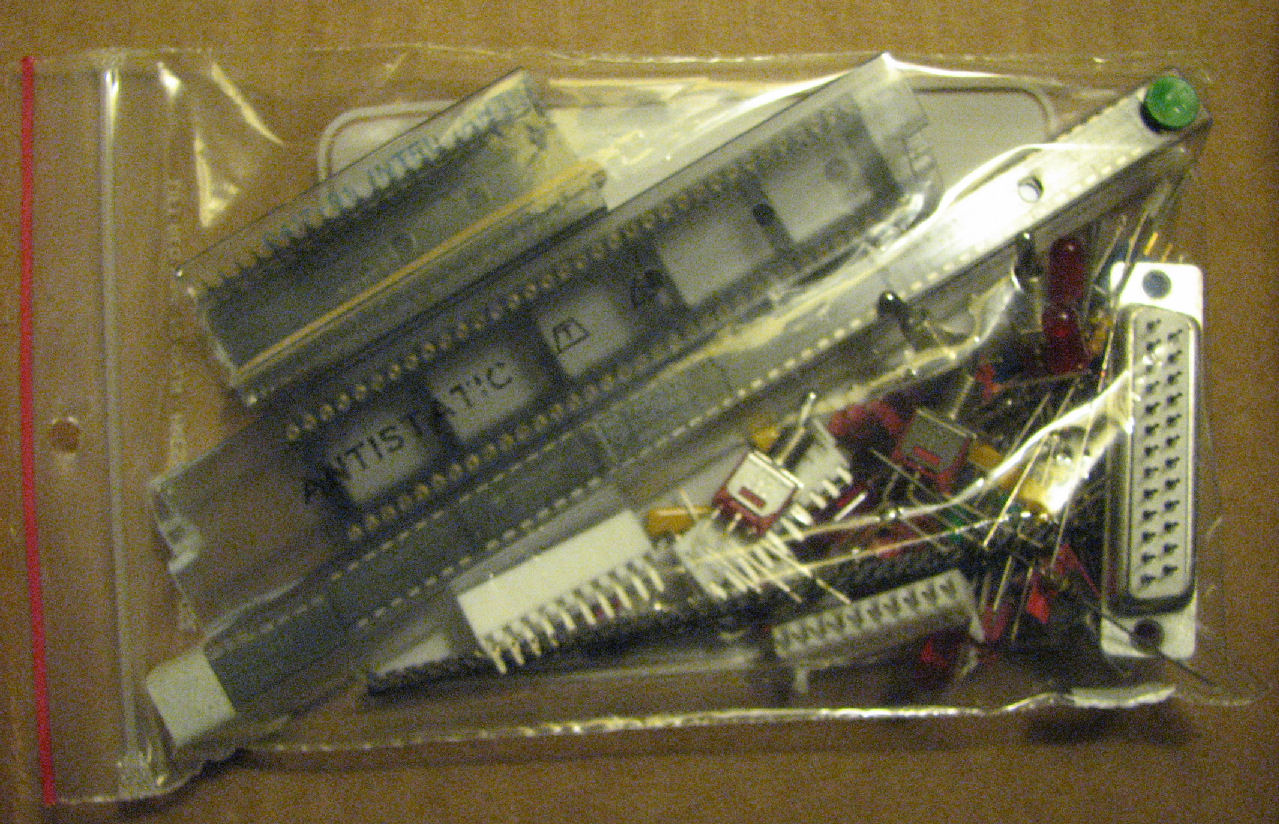
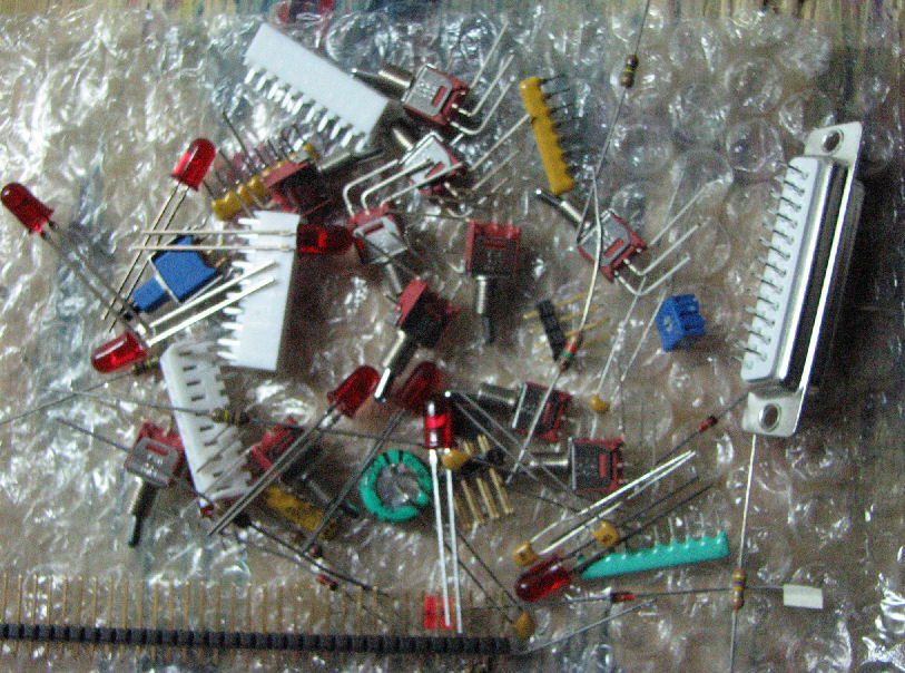
The parts bag, less some transistors
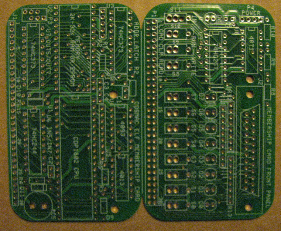
The circuit board.
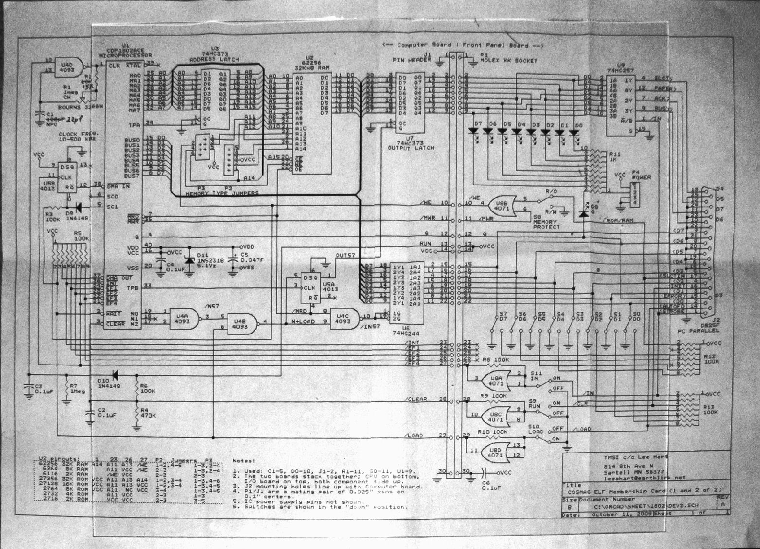
The schematic.
)(here's an updated PDF of the schematic)
The parts list.
Assembly of front panel
add DB-25
Assembly of CPU board
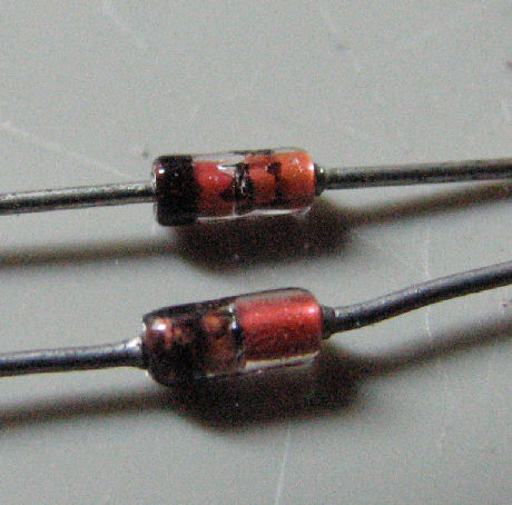
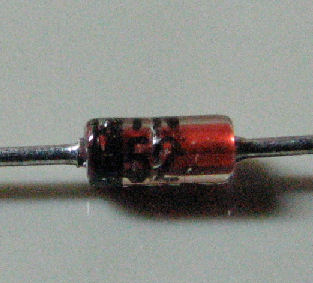
A challenge in dealing with these parts, is to identify them. Resistors have color bands which are readable by most; but many parts have extremely small text that are hard for many people to see. I used my digital camera to advantage, to get extreme closeups that I could also digitally magnify on my camera display. The diodes are a worst case of this challenge. Here's two diodes which I believed were the "signal" diodes. One is marked "41", corresponding to the 1N4148. The other was unmarked - likely to be another signal diode. Here's one diode that Lee marked with pieces of tape. It's marked "1N52", suggesting it's the 1N5231 or 1N5232 zener diode; another look found "31B" on the other side. The boards marks for the diode have a rectangle with a band at one end - this MUST match the dark-banded end on the diodes.
Feb 19th 2010: In brief, I spent a few hours over a few days to assemble the CPU board. Mounting these parts was simply a process of identifying them, mounting in correct position, and soldering and clipping leads. I found the "1M ohm" trimpot supplied was actually 100 ohms (by ohmmeter and by markings). Looked in my parts and junk for a substitute, but found none - so I substituted a 500K ohm resistor.
Before I inserted a part, I soldered any "through holes" that would be blocked by the parts. Don't rely on through-hole plating to survive without rust or cracking! Especially, don't rely on them to carry power - I learned in 1974 that "those are called fuses". All the open through-holes that did not get leads in them, were eventually soldered.
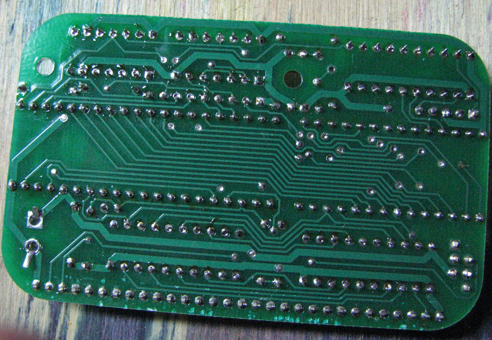
Here's a view of the assembled CPU board less the ROM and 1802.. To see the back of the board, here's the back of the CPU board. These digital photos provide a good opportunity to review parts, their position and to check solder joints.
![[assembled kit]](mship_comp.jpg)
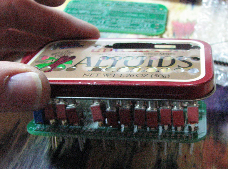
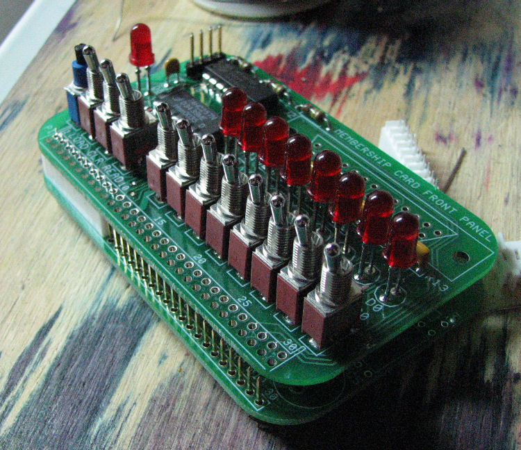
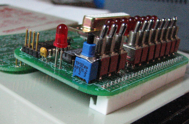
Here's the assembled 1802 Membership card, with a nickel to size it up.
March 5 2010: Here's a photo of the power supply and connector I made. This came from a 4.5V battery pack (3 AA cells); one of the pins is blocked off so I had to bend back one of the four power plug pins. If you look at the schematic, pins 3 and 4 are both ground, so I bent back pin 3 on the board's power pins, to accomodate the blocked jack as a "key". That's a good thing, now I have a "polarized" power plug!
The connector from the battery, had red and black reversed; it's not hard to bend up the tabs which hold the jack's pins in place and to move or add wires. Again, refer to the schematic and you will see pin 1 powers the chips (positive) but pin 2 grounds the pull-down resistors for the LED array.
I did not understand this, so I have a third wire from my power connector pin 2, which is grounded at my resistor pack. I think this is Lee's way to remove power from the LED's when the power connector is removed, so the on-board supercapacitor is not drained by LED current draw.
March: The card was assembled, but was not working. The LED's would at best blink ONCE on power up, but no toggling of switches would produce a pattern matching the data switches. I decided to check the activity of the switch OR gates (U8 on front panel board). see the schematic. to follow along what I did.
Sure enough, the IN, RUN or LOAD gates did not "toggle", except ONCE after power up and the switch was toggled. Also, the inputs to the gates "hung" at 1/2 the power supply level. I explained all this to Lee Hart; he initially assumed the OR chip was at fault and sent another one (and the 1MOhm trimpot for the clock circuit).
But I persisted in asking him why it would fail like that - and why of the four OR gates used for the control switches, the "read/write" OR gate which has a unique circuit from the other three DID work. Finally, I noticed an odd effect. When I put my finger on the input of a failed gate and the AC voltage level (from 60Hz hum) went above some point - the switch would "toggle"!
That got Lee's attention. He said "I think you put your finger on the problem." He decided the 100K resistor which is connected from input to output was too low; with the 100K network resistor to power, it divided the input level to a mid-way point neither high nor low. Increasing the "feedback" resistor allowed the input to become high enough to toggle the output when the switch was active.
March 22: I replaced R8 with a 470Kohm resistor as Lee suggested. The switch worked! So I replaced the other two resistors (R9, R10) with 470Kohm resistors, and confirmed they worked as well. Now, with some noodling of the switches, I could load values of some sort into RAM, and with more noodling I could see those values!
But the operation of the control switches is not obvious. Reading Lee's load test program instructions did not provide enough detail. And, I was not sure what memory address I was loading into. I contacted Lee, and he provided operating instructions which I'll apply next time. For reference to the switches, use this photo of the constructed front panel. Here's an updated PDF of the schematic.
March 24: I work through Lee's how-to-switch instructions and get familar with loading programs in the m'ship card. But his "blink the Q" doesn't work! I struggle to assemble the code and look it over...seems he had a bad branch. I figure out how to modify RAM rather than reload the program, fix the branch instruction. Lo, the Q LED is blinking! Ah.....And for even more fun, the code in memory only needed a patch because it stayed in memory, even after pulling out the battery. Now, *that's* how it gets done! (The code went away by the next morning, because the RAM consumes all of 20 microamps in standby. Lee says "true" CMOS 1uA RAMS are old and hard to find.)
When I told Lee Hart I got his programs running on my kit, he said: "I'm proud of you, Herb! I honestly felt a "tingle" of excitement, the same way I do when something I've worked hard on powers up and works for the first time! No kidding!"
Check the Membership Web page for the current status of the project.
- Herb Johnson
This page and edited content is copyright Herb Johnson (c) 2010. Contents written by Lee Hart, are copyright Lee Hart (c) 2010. Copyright of other contents beyond brief quotes, is held by those authors. Contact Herb at www.retrotechnology.com, an email address is available on that page..