![[RAM & CPU]](narrow_RAM_sch.jpg)
Last edit Dec 26 2017. Edited by Herb Johnson, (c) Herb Johnson, except for content written by others. Contact Herb at www.retrotechnology.com, an email address is on that page.
This Web page is about early 2017 testing of .300-wide DIP-packaged ROM on the 1802 Membership Card. The M/S Card accomodates both .600 inch wide ROM or RAM, and a .300 inch wide RAM under that chip. There's some .300-wide UVPROMs available - can they work with the M/S card? The issues include addressing, signal-pin differences, and current consumption.
Tests of 1802 Membership Cards at faster speeds and more current/power testing, is on this linked Web page. - Herb Johnson.
SInce revision G, the 1802 M/S CPU card has a concentric pair of RAM and ROM sockets. The wider 600-mil 24-pin socket, can accomodate either ROM or RAM. Lee Hart added to the PC board layout inside that socket, a 300-mil 24-pin socket, to accomodate a "narrow RAM" - typically a cache memory chip, used in old-school 80386 and 80486 PC's.
However, it's the case that some UVPROMs were produced in the 300-mill DIP case. They are uncommon, but available. In principle, they could work in that 300-mill socket. However, Lee Hart's layout for that socket "scrambled" some of the address lines; they are not in the expected order. That's no issue for RAM - all RAM is the same. But for ROM, it matters as they are programmed extrernally in address-order, by a PROM programmer. And, there's two other pins that need a fix: A14 and write-enable.
These considerations can be dealt with. Pins can be rewwired, and PROMs can be programmed to support a scrambled addressing. This Web page has notes and methods accordingly.
Note: check your manual and support Web page, for your version of the 1802 Membership Card CPU. Not all versions may support a narrow RAM/ROM, or have address lines scrambled.
Lee Hart, Feb 18-20 2017, private email: There's a "catch" with using an EPROM in a RAM socket on the Membership Card's 0.3" wide RAM socket. The pinouts are different between RAMs and EPROMs, [and need to be rewired] as follows:
PIN#	EPROM	RAM
-----	-----	---
1	VPP	A14
27	A14	/WE
![[ROM & CPU]](narrow_ROM_sch.jpg)
Additionally, due to layout constraints, the 1802MC address lines are slightly scrambled. This doesn't matter for a RAM; but it does matter for a ROM!
1802	U8 EPROM
----	--------
A0	is on A4 pin 6
A2	is on A0 pin 10
A3	is on A2 pin 8
A4	is on A3 pin 7
Anyway, this means you'd have to make a matching pin-scrambler socket adapter for your EPROM programmer, or pre-scramble the HEX file data in software that you burn into it, so things come out at the right addresses.
[An adapter, means] building a PROM-programmer adapter which scrambles the address lines. Then I can program and test these 0.3" wide EPROMs. When the program works, I can put the [programmed] chip in my EPROM programmer without scrambling the pins, read it, and save it to a file. Then, one can program that HEX file into their own 0.3" EPROM, without the adapter. [In other words,] It's a hardware way to scramble the data once, without having to write a special program [to scramble the address-order of the data].- Lee Hart.
Notes from Herb:A14 needs to be rewired; /WE and VDD do not. As for the A0-A4 addressing, the alternative to scrambling the PROM data address order, is to physically rewire the lines to the U8 narrow socket. That's a judgement call for the M/S owner. But it seems like more work and risk of damage.
Bill Rowe worked with the Cypress 27C256T-55WC from June 2017 forward. Thanks for his work and his notes. - Herb
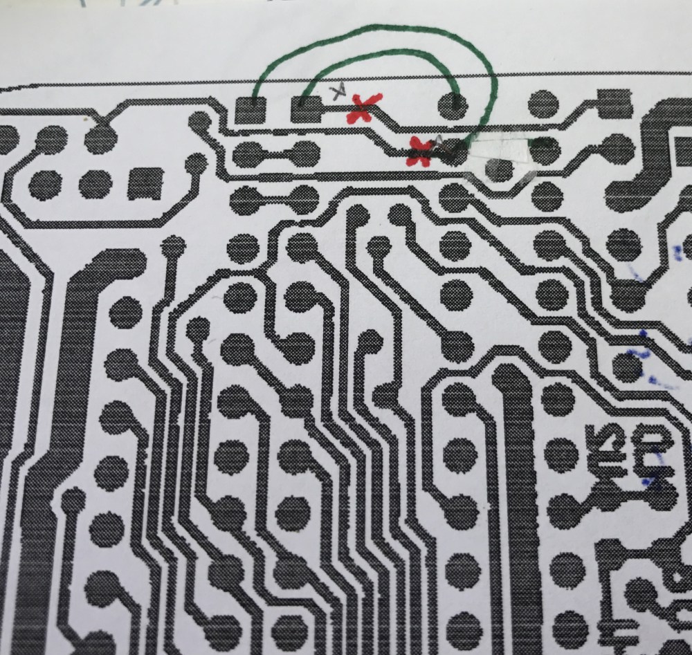
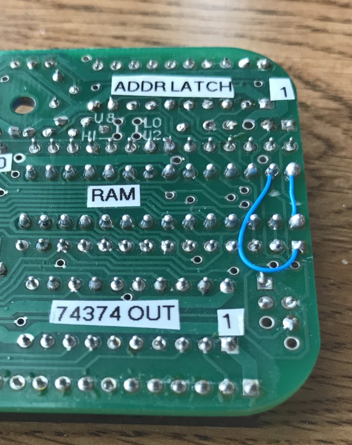
Pins 1 and 27 are easy to fix on the CPU board. Here's a view of the PC layout which draws those cuts and wiring. Here's a view of that actual wiring on the PC board. Thanks to Bill Rowe for this fix for a Cypress 27C256T-55WC, and these photos.
1) Josh was able to program it using his TL866CS programmer. You have to bypass the blank check because these erase to 0 rather than FF.
2) The parts are thicker/taller than normal memory chips. With the PROM in pin sockets at U8, U2 won't seat in a low profile socket above it. [Here's a photo.] You could use a higher socket for U2 but it might not fit under a front panel card (not a problem for me).
3) My rev G 4MHz CPU card has a faulty/slow /A15 circuit enabling U8, which causes [data] conflicts with the U2. [See clock discusssion later in this note. - herb]
4) The scrambled address lines can be addressed in software before burning the ROM or with an adapter [when buring the ROM]. I am seriously considering cutting the traces to the U8 and bridging to U2 with jumpers because it would be easy.
5) The Cypress ROM chips are power hungry as we knew going in. My specific interest is as a bootloader so I don't care. But I think they are drawing over 100ma [pending a fix to the /A15 problem]. - Bill Rowe
Bill reports in Sept 6 2017: "I finally(!) have one of the CY27256 packed in under an NVRAM on the Membership Card CPU board. I'm still just testing, so I have it in the default 0x8000 location and a long jump at location 0 in RAM starts my test code in the ROM. I put in an xmodem bootloader and some test sequences.
I used socket pins [in the PC board] to keep the ROM low. The tallest socket I could find for the RAM was a wire wrap socket. Given the tightness of the fit, it's really not that practical to be inserting and removing the narrow EPROM. I hope I only have to do it one more tine. [Here's a photo of Bill's board in profile.]
I have my own programmer now, a TL866CS from eBay which supports the parts, as long as you don't do a blank check. It expects 0xFFs for blank locations but the CY27C256 presents 00's. I made a wiring adapter [for the programmer, to work around the M/S card's scrambled addressing]. But it seemed to interfere with programming somehow. I ended up scrambling the addresses in software instead [by changing the addresses of the programmed data]." - Bill Rowe.
Bill will measure current draw later on. He erased the EPROM with eight days of "bare" sunlight exposure, so he reports. He's planning to make a different "Olduino" M/S Card version without an AVR processor, running the CPU at 4MHz. Follow his work at https://olduino.wordpress.com - Herb
Summary: In Oct 2017, I tested a 27C256 300-mil (narrow) UVEPROM in the M/S card. First, I tested the narrow ROM wired as a wide ROM in an adapter. Then I (re)built the adapter to unscramble the address lines, reprogrammed the PROM, and operated it as a narrow ROM, with a wide RAM. This took a lot of fuss. It may be simpler, to modify the CPU board, than to build all this apparatus! But you decide. - Herb
First: For testing the ROM in the M/S card, I wired up a narrow 28-pin socket atop a wide 28 pin socket. (Later I used this adapter for programming the PROM, that version is shown later.) I soldered the pins 15-28 of the narrow socket, directly to the same pins of the wide socket, since they would not be changed. That provided support for the narrrow socket atop the wide socket. Then I used wire-wrap wire and soldering, to wire up the pins 1-14.
Next, I set the CPU board RAM/ROM jumpers (to the wide socket) for a 27C256 EPROM. I programmed the narrow EPROM in the usual manner, for the IDIOT ROM monitor. With the narrow-ROM in the wide socket via adapter, and a narrow RAM in the narrow socket, I could run the IDIOT ROM monitor as normal. This verified the particular 27C256 EPROM would function in the 1802 board.
![[ROM & CPU]](u8prom_adapter.jpg)
Second: I rewired the adapter to change the scrambled addresses, so I could program the PROM
without "unscrambling" the addresses on the CPU board. (In fact it took two tries to rewire the
adapter.) Here's the wiring scheme needed between the narrow socket and the wide socket:
       narrow	wide
	6	10
	9	9
	10	8
	8	7
	7	6
Next: I erased and programmed the 27C256, in the adapter I just described. My PROM programmer
wasn't happy with a scrambled EPROM; it did not see the "signature" that many modern PROMS have
internally and that "check" had to be "ignored".
![[ROM & CPU]](u8prom_pin27.jpg)
Third: Before I used the PROM in U8, I had to make a physical change to the PROM, on its pin 27 for the PROM's A14. I bent the PROM pin 27, to keep it disconnected from
the U8 socket pin 27. And, I soldered a wire from the disconnected pin 27, to the PROM's pin 1.
In the U8 socket, pin 1 is A14. On the PROM, pin 1 is Vpp, the programming pin - it doesn't matter
that it's on A14.
![[ROM & CPU]](u8prom_2chips.jpg)
![[ROM & CPU]](u8prom_stack.jpg)
Fourth: With the modification to the PROM, I could now insert it in the narrow socket U8. Then,
I could re-jumper the U2 socket for RAM, and insert a 62256 wide RAM in U2. Looking at the photo,
the very tall U8 PROM, keeps the wide U2 RAM from full insertion into the wide U2 socket. I used inserted PC board pins for the narrow socket. Pay attention to this problem of "clearance" for your choices of PROM, RAM and sockets for each.
For all this fuss, I was able to run the IDIOT ROM monitor from the narrrow ROM and wide RAM. - Herb Johnson
Somewhat related to ROM vs RAM, is CPU clock speed. Those who experiement with both ROM and RAM, or faster CPU clock speeds, may see problems with A15 ROM/RAM selection. The issue, in short, is the speed of operation of the /A15 logic inverter. Various versions of the 1802 M/S card use different circuits. Read this Tech Note about REv G circuits and fixes to it for details. For versions which use a single FET or transistor for /A15, the pullup resistor must be reduced from 100K to 10K, or to a few K ohms. Versions after Rev G, use a N-channel plus P-channel MOSFETs as the inverter, no pullup; or other schemes. They operate faster and use less current too. Thanks to Lee Hart for some of this discussion.
This page and edited content is copyright Herb Johnson (c) 2017, execept content written by Lee Hart or Bill Rowe, for which they have copyright. Contact Herb at www.retrotechnology.com, an email address is available on that page..
![[Here's a photo.]](rowe_17-06-21-room.jpg)
![[Here's a photo of Bill's board in profile.]](rowe_17-09-06.jpg)