CHIP	Rev G	Rev I		Rev I+ (to 8MHz only)
1	4Mhz	6Mhz	4Mhz
2	8Mhz	4MHz	6Mhz
3	7MHz	4MHz	4MHz   funny clock behavior
4	2MHz	10Mhz	8+Mhz     Rev G triangular clock at 4Mhz
5	6Mhz	10Mhz	8+MHz
Observations during 4.5V testing
CPU #3 had trouble producing a good clock. On the Rev G board, the 8Mhz ceramic produced a 7Mhz clock. On the Rev I board, I got IDIOT operation on the 6Mhz ceramic by tweaking clock down to 5Mhz but it eventually jumped to 6Mhz and IDIOT failed. In OCt tested ten on rev I, various date codes. 8 ran to 4MHz, 1 to 6Mhz, 1 to 2Mhz.
CPU #4 on Rev G board, produced a rounded-triangular clock at 4Mhz, but was square at 2Mhz. On the Rev I board in Sept, the 8Mhz clock was a little "pointy" but opeated OK, but only tested one. In Oct I tested ten of these on Rev I; nine ran to 10Mhz, one to 8Mhz, one to 6Mhz.
Rev G tests in Sept were limited to 8Mhz clocking. But Rev G tests in Oct with a Harris chip or RCA chip, only oscillated to 4Mhz.
Observations about TPA and buffering (4.5V)
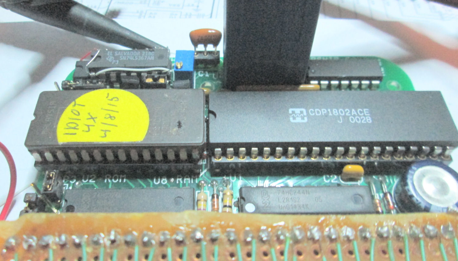
![[74ls367 mounted]](1802_speed_3541.jpg)
I first tested Rev I, with a pair of 74LS367 buffers in series with the TPA signal, to 8MHz.
The 74LS367 was mounted atop the 74HC373 address latch, and buffers to TPA wired in. Details of wiring are elsewhere in this document. Later, I removed the TPA buffers from the circuit, and tested to 10Mhz. CPU chips which failed at 4MHz or 6MHz with buffered TPA, ran slower or faster to 4Mhz or 6MHz. Chips which succeeded to 8Mhz with TPA buffered, ran at 8Mhz and also at previously-untested 10Mhz when TPA was unbuffered. It's unclear to me, there's a benefit of buffering TPA at 10Mhz clock or below, when you can instead choose higher-performing 1802 CPU chips. - Herb
Observations of TPA and clock
Rev I without TPA buffering, 4.5V
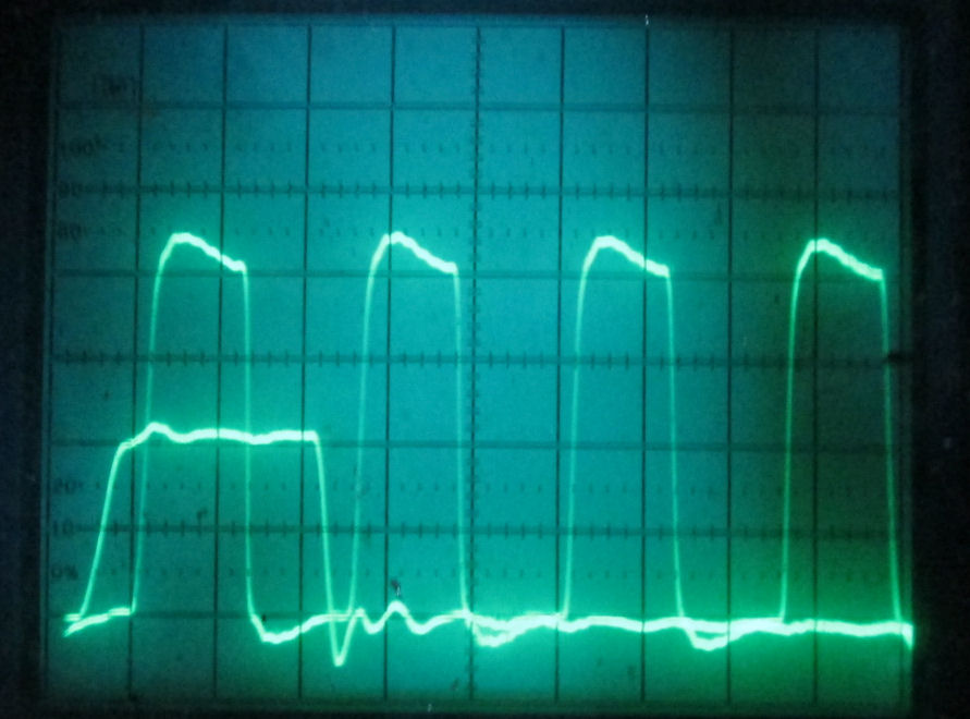
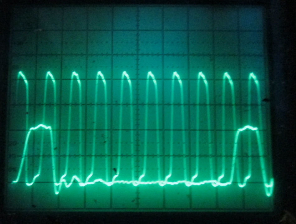
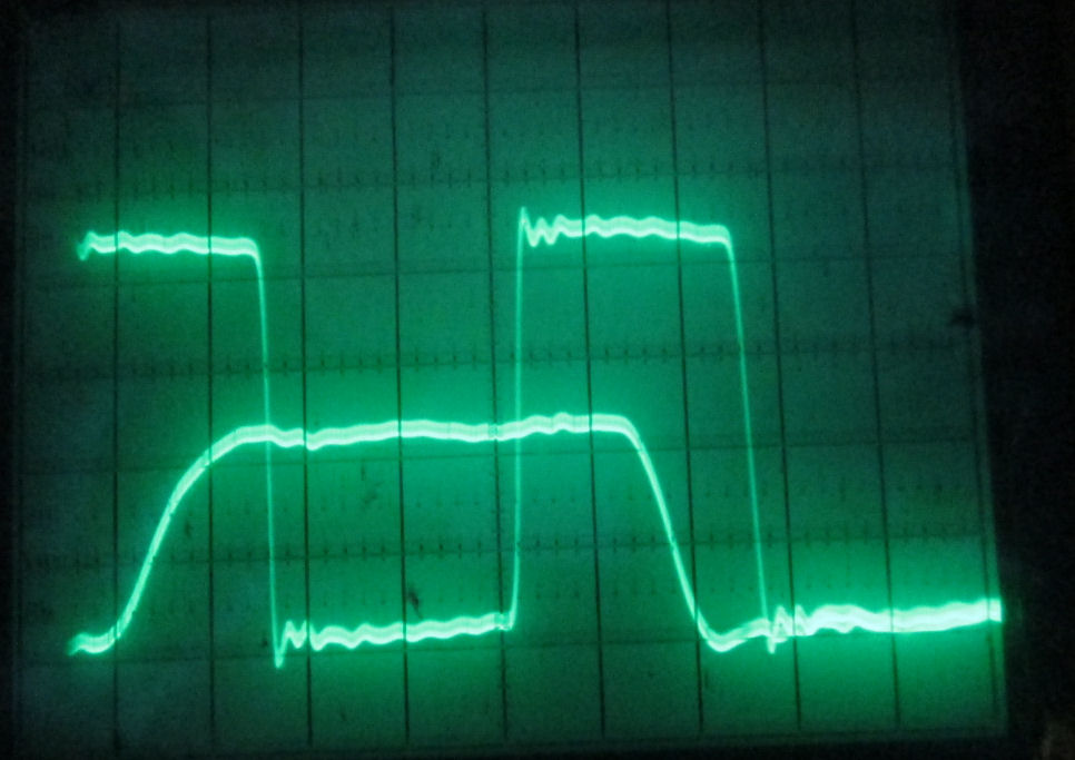
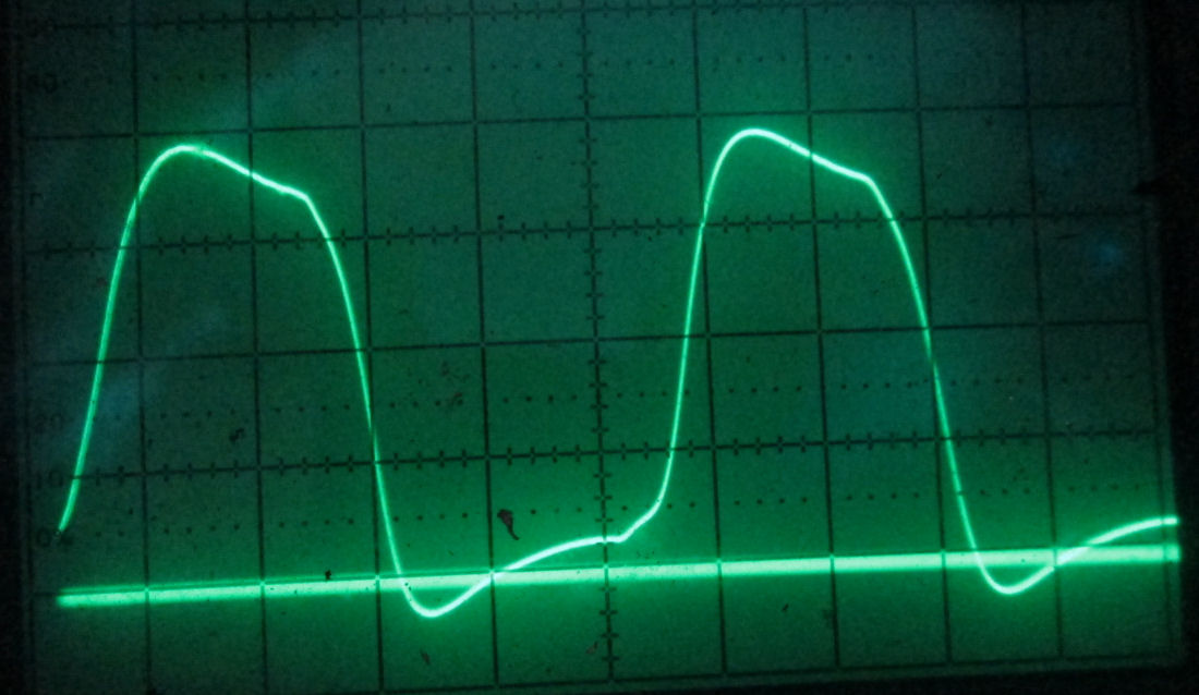
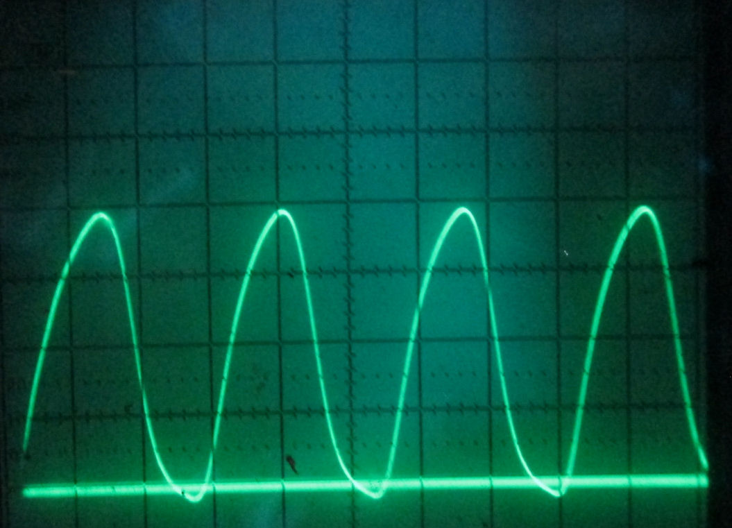
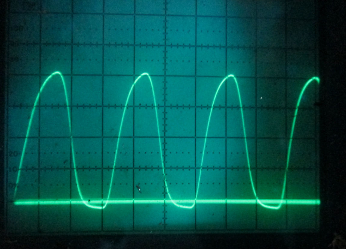
Conditions: substitute ceramic resonators from 4-10Mhz. 3983 - CPD1802ACE J 0028 Harris chip (#5) under test. Buffer disconnected on TPA. Clock is 74HC138. Battery supply 4.4 to 4.5 volts. 50Mhz oscilloscope monitoring TPA and clock with 10X probes. TPA shown at half level of clock. Horizontal scan rate 1Mhz (100ns/division), sync on TPA. TPA bounce past trailing edge may be due to poor grounding of scope probe.
3988 - 10MHz clock and TPA, trimpot re-adjusted to click, back 1 turn
3990 - 10Mhz clock, scan at 2Mhz, and synced on TPA. TPA and clock at same vertical scale.
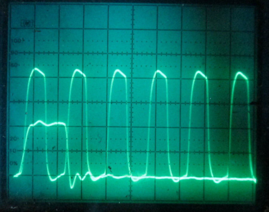
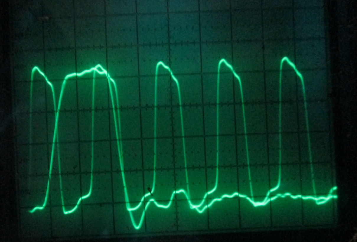
Rev I with TPA buffering, 4.5V
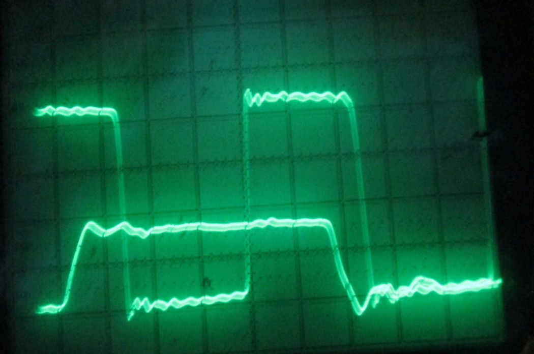
CPU is RCA CPD1802CE RCA 223 R, plastic. Rev I, with one or two 74LS357 buffers on TPA. Various clock speeds. View of TPA before and after buffers, shown at half vertical scale from CPU clock. Oscillograms at different horizontal scans.
3541 wired 74LS367 over 74HC373. disconnected pin 11 from TPA, wired TPA through one buffer on '367.
3546 6MHz clock, TPA before buffer at 1802 and clock, displayed 50ns/div, TPA spans over 200ns, but >50ns rise time and 40ns fall time.
3547 TPA after '367, note faster rise and fall times buffered TPA 30ns rise, 20ns fall, spans 200ns, hard to determine propogation delay in LS367.
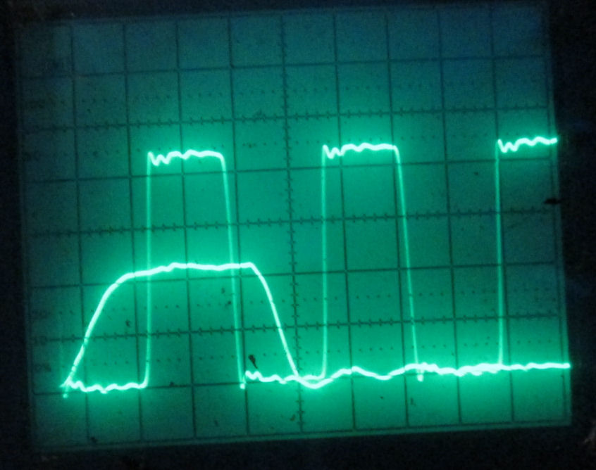
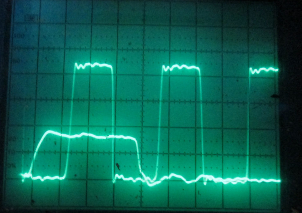
3548, 3549 added second '367 delay, TPA from 1802, 6Mhz, 25 ns/division.
3550 TPA after second '367. TPA now spans 300ns, rise time 30ns, fall time 20ns.
Results of 6Mhz buffered operation: no change! can't run IDIOT at 6Mhz, TPA buffered or unbuffered. But later, I tweaked CPUT clock and ran IDIOT at 5Mhz. Conclusion: Problem is not TPA, but excessive 6MHz clock speed for CPU.
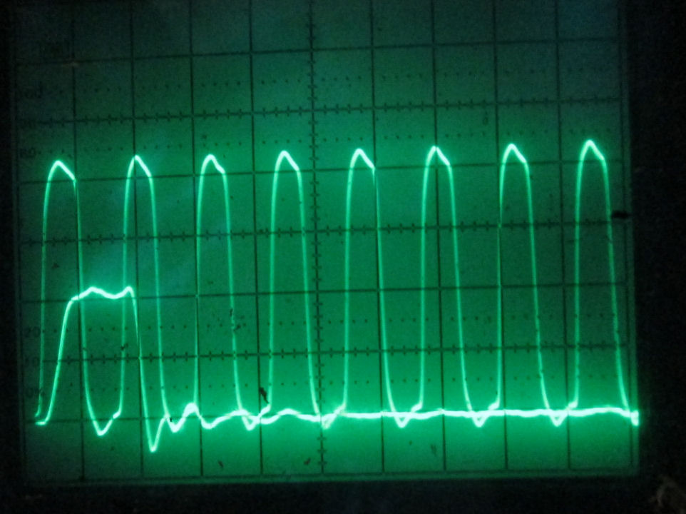
Rev G clock, 4.5V DC supply
Tests with Rev G CPU with transistor for A15 inverter, and 4093 gate for oscillator. CPD1802ACE J 0028 Harris chip (#5). Battery supply 4.4 to 4.5 volts. 50Mhz oscilloscope monitoring TPA and clock with 10X probes. Horizontal scan rate 1Mhz (100ns/division), sync on clock
3995 - CPD1802ACE J 0028 Harris chip under test on Rev G.
3998 - 4Mhz clock - looks triangular
4000 - attempted 6Mhz on Harris chip, clock looks like 3.5Mhz. approx. same result occurred with RCA 1802 chip.
Details of boards and modifications
Replacing the 4093 with 74HC132
![[U4 replace]](1802_speed_3473.jpg)
Here's the changes needed to replace the U4 4093 with a 74HC132. Both the 4093 and 74HC132 are four 2-input NAND gates. For replacement: 3473 identifies that connections to pins 4 and 6 must be exchanged. and connections to pins 10 and 8 must be exchanged. Lines to these pins come from U4 itself, U5, and U6. In the sketches and photos that follow, keep in mind if the view is from the top (component side) or the bottom (solder side). Note the three feed through holes of U4, to orient your view.
![[U4 replace]](1802_speed_3400.jpg)
![[U4 replace]](1802_speed_3402.jpg)
Here's the PC board area of U4. 3400 is the bottom of the
CPU board, the U4 4093 socket area is to the right, U5 is to the left. 3402 is the top (component side) of the CPU board where the 4093 is mounted, socket-pins in place. U5 is to the right and soldered in place. NOte the three feed through holes in the 4093 U4 area.
![[U4 replace]](1802_speed_3468.jpg)
![[U4 replace]](1802_speed_3472.jpg)
Here's sketches of the PC board cuts and rewiring. 3468 is a sketch of the PC board traces around U4. The X's show the cuts on the bottom (and top by dotted line) of U4 socket 4093, and routing to U5 and U6. 3472 shows the top (component side) view of new wiring to U4.
![[U4 replace]](1802_speed_3467.jpg)
![[U4 replace]](1802_speed_3465.jpg)
Here's the PC board cuts around U4. 3467 shows the U4 socket traces on the bottom which were cut. 3465 shows the U4 socket traces on the top, which were cut. Note the three feed through holes of U4. The U6 trace cut from U4 Pin 10, will be soldered to later, you will have to scrape it
to bare copper.
![[U4 replace]](1802_speed_3471.jpg)
![[U4 replace]](1802_speed_3470.jpg)
Here's the wires added around U4. 3471, shows the wires added to the bottom of U4. 3470 shows the wire added to the top of the U4 socket area; note it's soldered to the cut-off trace. NOte the three feed through holes of U4.
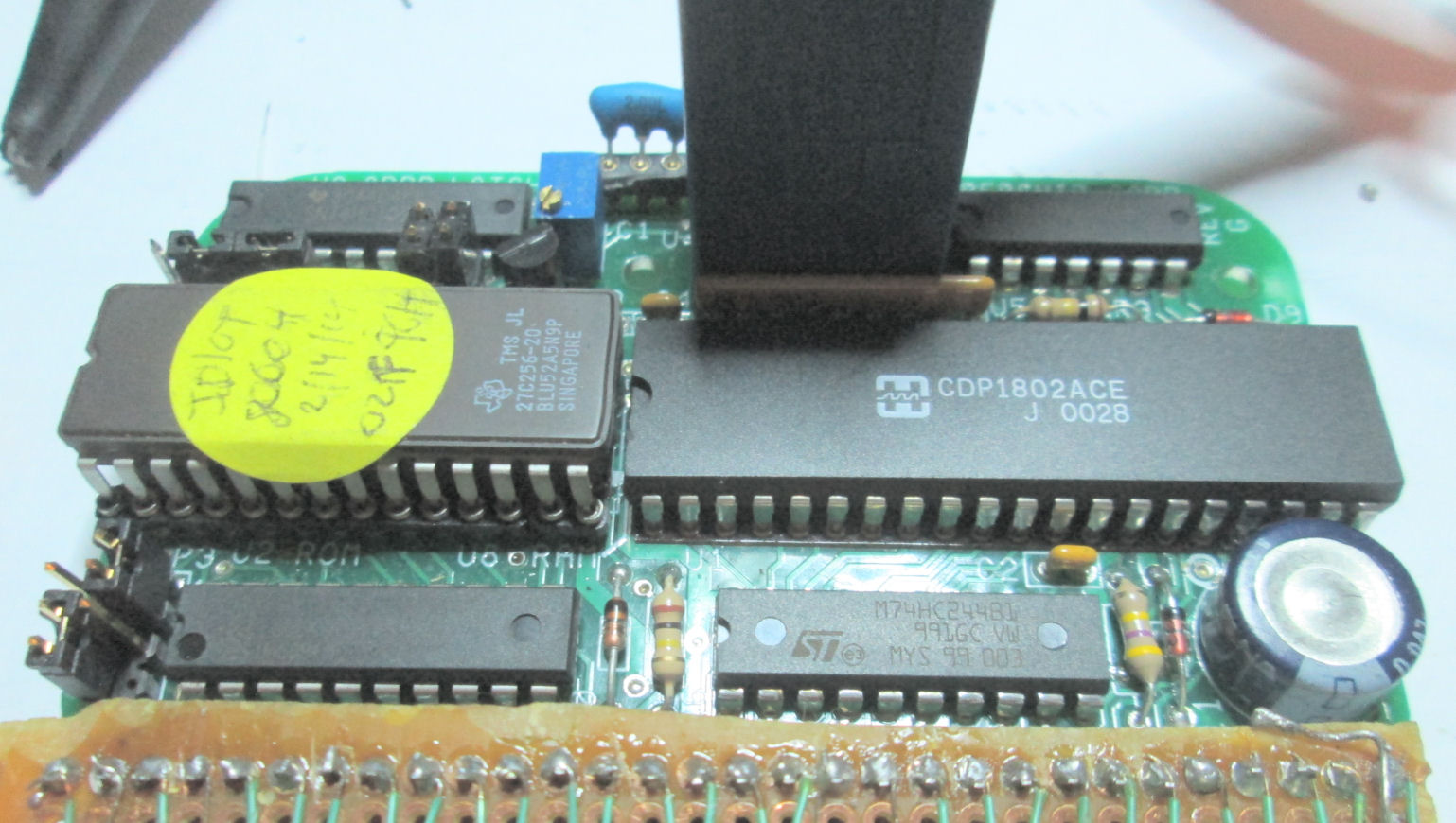
Mounting the TPA buffer atop the address latch
![[74ls367 mounted]](1802_speed_3541a.jpg)
![[74ls367 mounted]](1802_speed_3548.jpg)
The details of mounting the 74LS367 atop the 74HC373 address latch are these. The 74LS367 was mounted to the top of the '373 address latch. Pin 8 of the '367 was soldered directly to pin 10 of the '373 latch (grounds). pin 16 of the '367, was wired (red) to pin 20 of the '373 address latch (Vcc). Pin 15 of the '367, was wired (bare) to pin 1 of the '367, and both wired (white) to pin 8 of the '367 (grounding the enable of the '367 buffer). 3541a shows the '367 on the pin 1 to 8 side and 3548 shows the '367 on the pin 16 to 8 side
HEre's the details of wiring in the TPA signal. 3548 shows the area where TPA is wired The '367 is mounted above the '373 address latch. MOst of the pins on the '367 buffer are cut short, except for pins to be soldred directly to the '373 latch underneath it. Other connections are by short wires of various colors. Look at the photos in this section to see the chips and wires.
Pin 11 of the address latch is connected to TPA from the 1802. I broke that connection by cutting pin 11 at the IC. I soldered a wire (white) to the pin 11 PC board hole, and wired it to pin 10 of the '367. For one buffer, the TPA wire was connected to pin 11 of the '367. For two buffers, I wired pin 11 of the '367 to pin 10, and wired the TPA wire to pin 9.
Removing the '367 from use was simple. Just desolder pin 8 from the '367 buffer, from pin 11 of the '373 latch. and, move the (white) wire with the TPA signal, from the '367 and back to pin 11 of the '373 latch. Or later, remove the entire '367 and solder-bridge pin 11 of the '373 address buffer back to its pin 11 hole.
Current consumption, DC voltages and speeds
Conditions: Rev I CPU board with 74HC132, CDP1802CE RCA 223 R, Rev B/C front panel, with no LED's on except Q. AM27C128 ROM, GLT7256M08-15T 300 mill 32K SRAM. 3 AA batteries 4.4V to 4.5V.
"wait" is waiting for character input - mostly running ROM
"ROM/RAM" is dump of ROM - some RAM access, serial out current
"DMA" is in LOAD state, enabling RAM output constantly, serial ??high ??low
Current measured with Simpson 260 analog meter on 120mA scale, at DC power supply.
Ammmeter may have dropped voltage to 1802 test system.
Results:
speed  DMA   ROM/RAM  wait
2MHz    55     24      21
4Mhz    55     26      21
6Mhz   58-60   30/31   crashed
Conditions: Rev I CPU (74HC132) + six CDP1802CE RCA chips 1981-1983,
Rev B/C front panel, with no LED's on except Q.
AM27C128 ROM, GLT7256M08-15T 300 mill 32K SRAM.
Simpson 260 analog meter at 120mA DC scale in series with 5.0V DC supply; delivers 4.91-4.93V to 1802 boards.
Results:
2MHz
wait 15  17  15  16  15  15  15
DMA  65  60  62  60  60  58  59
ROM  20  21  21  21  21  20  21
RAM  21  21  21  21  21  21  21

4MHz
wait 17  17  18  18  18  17  17
DMA  62  62  62  61  60  56  59
ROM  22  23  23  23  23  22  23
RAM  22  23  23  23  22  22  23
Notes: when first powered up, current a few mA higher; drifts down slowly over several seconds.
Conditions: as above but clock frequencies were 4Mhz, 8Mhz, 12Mhz. CPU chips tested were Harris brand H9740 and J0028, previously ran to 12Mhz.
Results:
H9740   4Mhz  8Mhz  12Mhz
idle    17    21    24
DMA     60    63    64
ROM     24    27    32
RAM     23    27    32

J0028   4Mhz  8Mhz  12Mhz
idle    17    21    25
DMA     61    62    64
ROM     23    27    32
RAM     23    27    33
Note. Four H9740's and three J0028's were tested at 4Mhz. Results were within 1-2mA.
NOte. When "cold" (first inserted into board) the DMA current was several mA higher. It sank over the course of about 20 seconds to the lower value reported. DMA current seemed stable after less than a minute under power.
Comparison with other narrow RAM tests
The dominant current consumption in these tests, is by the 300-mil wide GLT7256M08-15T RAM. Designed for 80486 cache speed, they use high-current data output drivers. On "DMA", the RAM is always enabled and its output drivers are active - for maximum DC current.
For a comparison of various RAM-cache chips, check this linked Web page of 1.8Mhz tests of many 300-mill RAMs on a Rev-G Membership Card. Those tests suggest the Rev G card set and CMOS ROM consume about 16mA at 4.4-4.5V DC. Tests on this page at 5.0V & 2Mhz, shows about 21-22mA. Again on the linked Web page, the GLT7256M08-15T runs a RAM-only program at 44mA at 4.1V DC. Meanwhile, the tests on this Web page at 2Mhz, DMA operation of RAM was 60mA at 5.0V DC. These are roughly consistent given differences in DC power and mode of operation. - Herb
Herb Johnson
New Jersey, USA
check my ordering page to send email @ me
Copyright © 2017 Herb Johnson