Last updated July 13 2019. Edited by Herb Johnson, (c) Herb Johnson, except for content written by others. Contact Herb at www.retrotechnology.com, an email address is on that page..
Problem: In June 2019, I was asked about problems with a Digital Systems brand of floppy-disk drive controller (Rev 3.3) and its S-100 bus interface (HB 1.3). Timothy Colegrove, the new owner of that controller and IMSAI computer, could "boot" a CP/M diskette supplied with that system. But he could not write or format another diskette. He was in email contact with me, and with several other people including Jeff Shook (who owns a DS System on an IMSAI) and Larry Greene.
Background: Digital Systems made a very early 8-inch floppy disk drive controller, and sold a S-100 (IMSAI/Altair bus) "buss interface" card for that controller. I discuss that controller and provide documents on this linked Web page. Near the bottom of the page, is a section "Digital Systems FDC documents, software, images of hardware". THere's a number of ZIPped and PDFed documents and software there. I've acquired, a number of versions and revisions of that floppy controller, a few revisions of the buss interface card; and I have limited documentation for them as I've provided.
From the documents I have available, plus tracing the circuits (visually, ohmmeter, decoding the logic) on the two cards in hand, I have some partial information on how the DS controller and buss interface manage "write protect" for the attached floppy disks drives. This is work in progress, may be incomplete, and may have errors. As I'm writing as I go along - to show you what such work looks like.
Tentative result: reviewing revision 3.31 of the FDC (floppy controller) board, I found circuits which can force "write gate" to the drives (drive pin 40 J3) to become disabled. There's a jumper area to accomplished this, to prohibit writes to all drives. That's a different operation than described for earlier documentation (revision 1? December 1976) of the controller, which shows and describes a jumper to prohibit writes to drive 0 only. The notes, photos and drawings below describe these features. Later, I found I had confirming documentation for revision 3 of the FDC. The ZIP file which I say has "Documents for FDC 3.3 and HB 1.4 is at this link. In that file is "Dig_Sys_FDC3.pdf", relevant for the hardware I was examining today.
I was not able at first, to "trace" sensibly, a "WP" jumpered line from the S-100 "buss interface", through pin 50 of the connecting cable, to circuits on J1 of the revision 3.31 FDC board; there's no connection described to pin 50 J1, for the "December 1976" documented FDC-1. But laterI did find a connection in documentation for revision FDC 3.3; it's a 20MHz signal from the FDC clock circuit, to the S-100 board. My traced schematic, was correct but incomplete. Whatever the purpose of that signal; it's not a write-protect signal. - Herb
- Herb Johnson
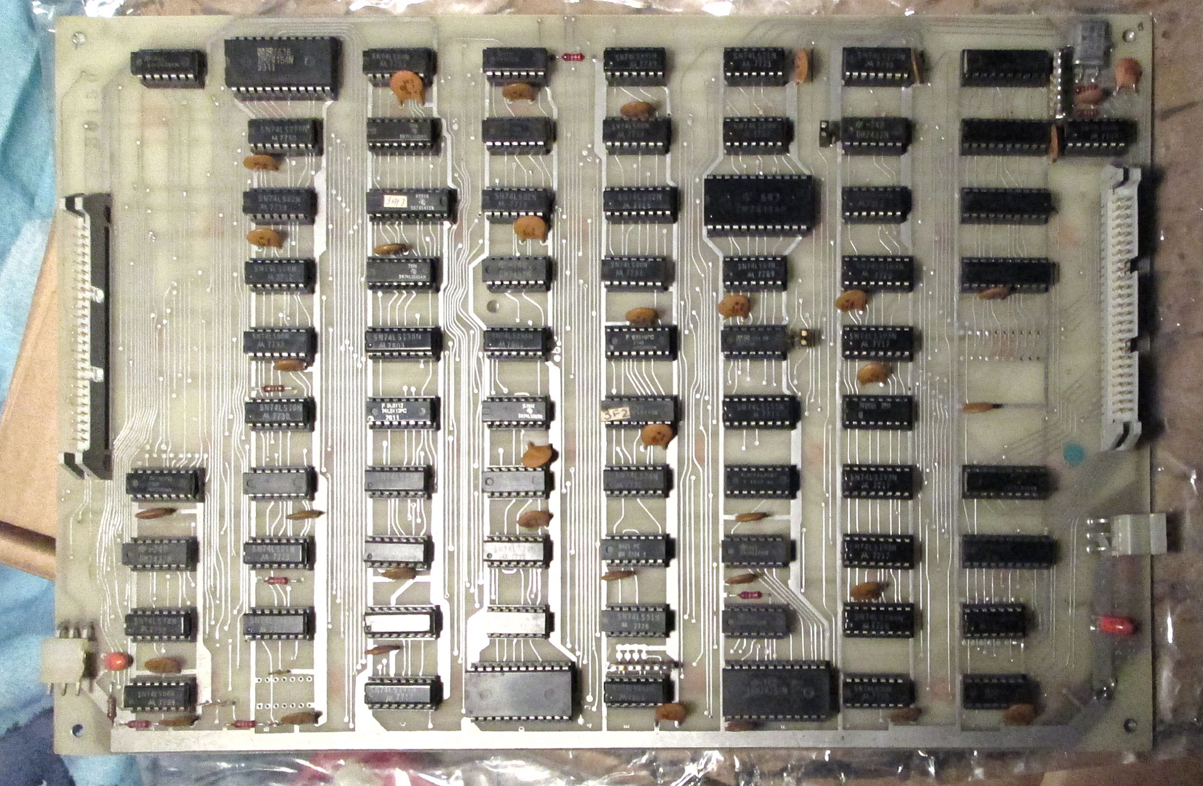
Linked is an image of a revision 3.3 A of the Digital Systems floppy drive controller board. I discuss that controller among others, and provide documents, on this linked Web page. Near the bottom of the page, is a section "Digital Systems FDC documents, software, images of hardware". A list of linked documents follows.
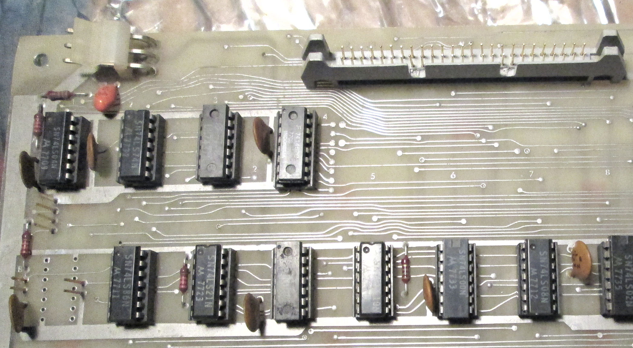
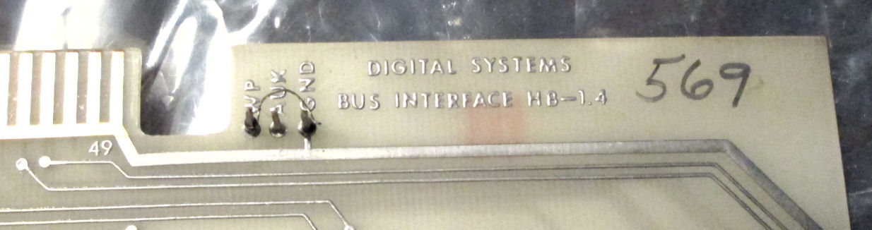
Linked is an image of the 3.3A "J1" connector which connects the board to the "buss interface card". The board's identifying information is shown.
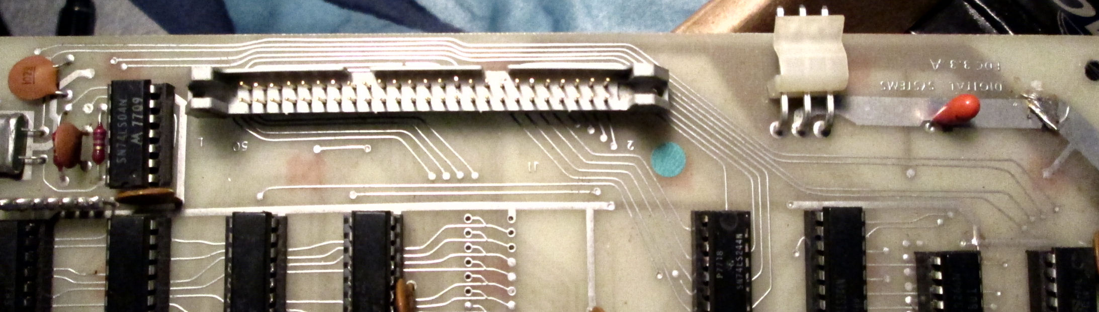
Linked is an image of the 3.3A "J3" connector which connects the controller board to the two 8-inch floppy drives. I assume the drives are Shugart 800/801 drives. Those are single-sided, single or double-density capable drives. I believe the DS controller doesn't support double-sided drives (or diskettes).
Among the ZIPped documentation available on this linked Web file, is a "Digital Systems Model FDC-1 floppy disk controller interface manual" for 1976. Schematics are dated 12/76. These schematics and manual, don't correspond to the 3.31 version of the FDC which is shown in this discussion: I determined that later. But it's the documentation I have.
Here's a relevant exerpt of that manual. It consists of the title page, the schematic. This manual has schematics for a FDC-1 drawn 12-76 (Dec 1976).
PDF page 18 of the full disk-controller manual, has a section titled "WRITE PROTECT". quote: "The FDC provides write protection for the disk drive selected by signal -DS0 or all drives (jumper selectable). In order to allow writing, the DZPROT signal on J1-9 must be grounded (TTL "0") by the host system." Note, this is describing the floppy-controller, not the host-interface AKA buss interface. I'm looking at this manual's schematic for J1 pin 9.
On PDF page 6, is the upper half of sheet 3 of the FDC-1 schematic. Look at the upper left corner *of the PDF page* - corresponding to the upper-right corner of the schematic when properly oriented. There's a 7400 NAND gate with location information "B11". Pin 1 has a 1K pullup resistor. The line continues to a designation "J1-9" connection. There's a notation "(normal)". There's a jumper noted, at pin 2 of B11; to short to pin 1 of B11; or to connect pin 2 of B11 to the output of B12 (inverter or gate) pin 8. There's a description: "possible jumper". Pin 9 of B12, connects to "DS0 J3-26". Pin 25 of J3 is the floppy-drive "disk 0" enable line (active low). J3, is the connector to the floppy drives.
B12 the gate, a 7437, has an input pin 13; follow that line on the schematic and it goes to a signal "WG" from flip-flop D1 pin 9. B12 the gate, also has an output pin 11, to J3-40. Any available Shugart manual shows Pin 40 is ... Write Gate! The signal that when low, enables disk write.
I conclude from the schematic, that the jumper near B11 provides an option, to disable "write gate" when drive-select 0 (the boot drive) is active. In other words: to disable disk-writes to the boot-drive 0. This confirms the documented statement.
Look again at the area near J3 of the 3.31 FDC. Again, that's where the floppy drives are connected. So we learn from the above information, that pin 40 is the drive's "write gate". I manually traced, by eye and ohmmeter, the signal line from J3 pin 40.
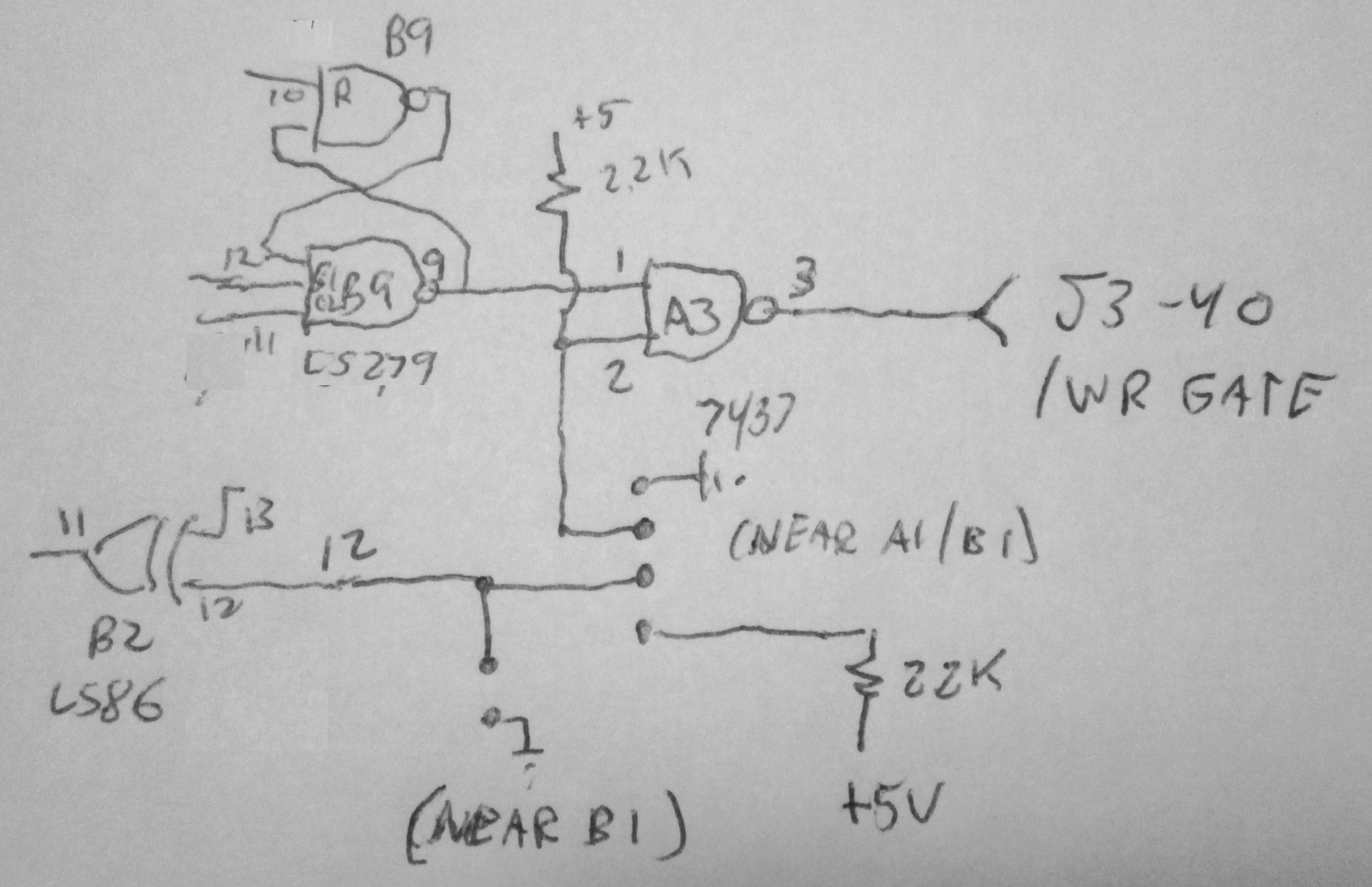
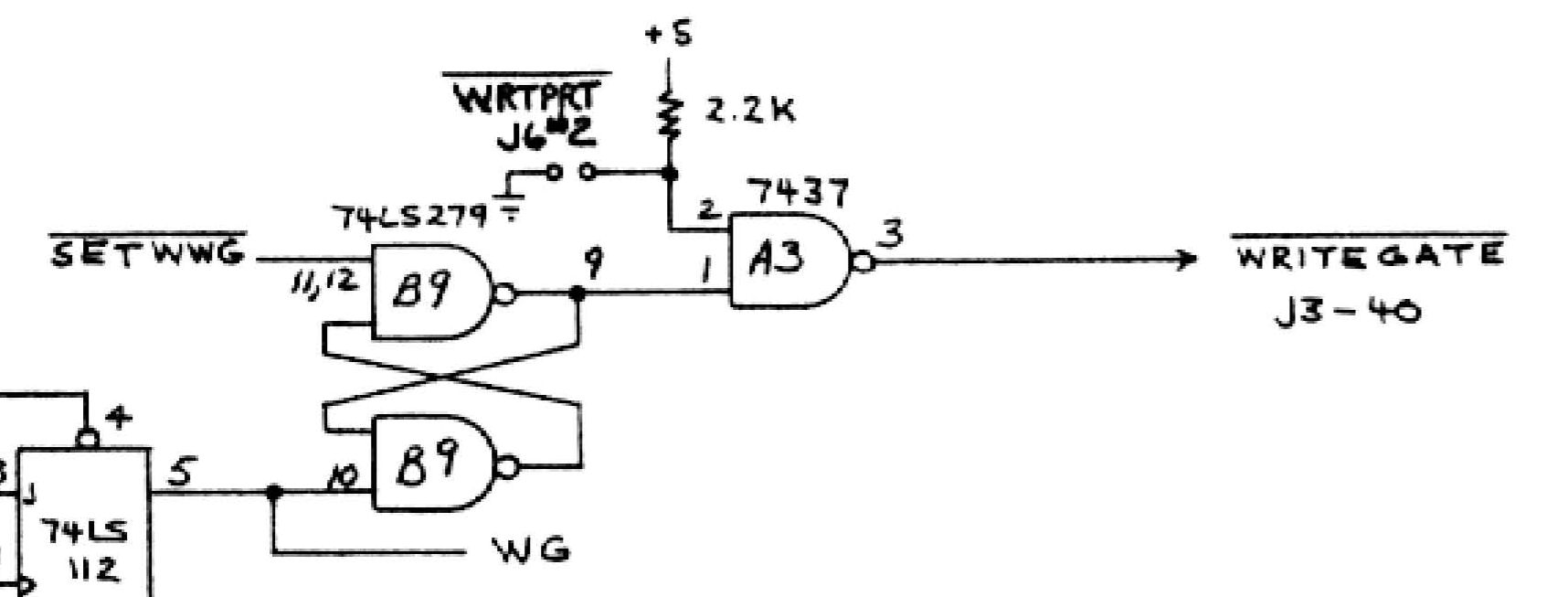
Here's a hand-drawn schematic for the circuit which drives J3 pin 40. Again, this is version THREE of the controller; the documentation described above was for a different and earlier version. Tracing the circuit, I see that pin 40 is driven by a 7437 gate at board location A3, pin 3. Pin 1 of the gate connects to the R-S flip flop output of 74LS279, pin 9. Presumably that is the "write gate" signal. Pin 2 of the gate A7, is pulled up to 5 volts by a 2.2K resistor. The line also goes to one of four jumper pins, located near chips A1 and B1. Adjacent to that pin is a ground pin.
Pay attention! If pin 2 of the gate A3 is grounded, gate A3 output will NEVER GO LOW. That is, it will inhibit "write gate" from becoming active. NONE of the drives connected to the floppy controller, will be able to write (or format) to a diskette! So Pin 2 must be "unjumpered to ground" to permit disk writes.
There's additional pins in the jumper area, but I don't believe they are relevant for write-protect. The remaining two jumper pins, of the set of four, connect chip B1 (74LS86) pin 12 (input to an exclusive OR gate) to another 2.3K pull-up resistor - it will pull the line HIGH. In addition, there's a jumper near chip B1 of two pins. That jumper, if shorted, will GROUND pin 12. The nature of the exclusive OR gate, is such that one of these two jumpers will either invert, or not invert, the logic signal from pin 13 input to the B2 located 74LS86, to the output pin 11. I did not investigate the details of this signal.
The ZIP file which I say hsa "Documents for FDC 3.3 and HB 1.4 is at this link. IN that file is "Dig_Sys_FDC3.pdf" with a schematic for FDC 3.3 disk controller, and HB 1.4 S-100 buss interface. And, good news! sheet 3 of 3, shows the write-gate J3-40, and /WRTPRT jumper J6 #2; as I've drawn them! Here's that portion of that schematic.
Later, I looked at the revision 3.3 FDC schematic, for any format disable jumper. Sometimes floppy or hard-drive controllers have such options. From a read of the 3.3 FDC schematic, "format" operation seems to be enabled (gate 7B) by two signals, "format" and "formatenbl". Each comes from a bit from a register which is set by software: no obvious jumper.
But in July 2019, based on a tip from Dwight Elvey, I looked at the schematic again around the ROMS. And on sheet 2 of 3, I see the , "format" and "formatenbl" signals to gate 7B pins 1 and 2; pin 3 goes to pin 19 ROM C8, a 74S472. That's address line A8 which would select another half of the 512-byte ROM. Thus the version 3 FDC, has half a ROM devoted to disk-format, as selected by control bits of the FDC.
There's a suspicious jumper on one of my S-100 buss-interface boards, that suggests it has something to do with "write protect". Here's what I figured out, and how.
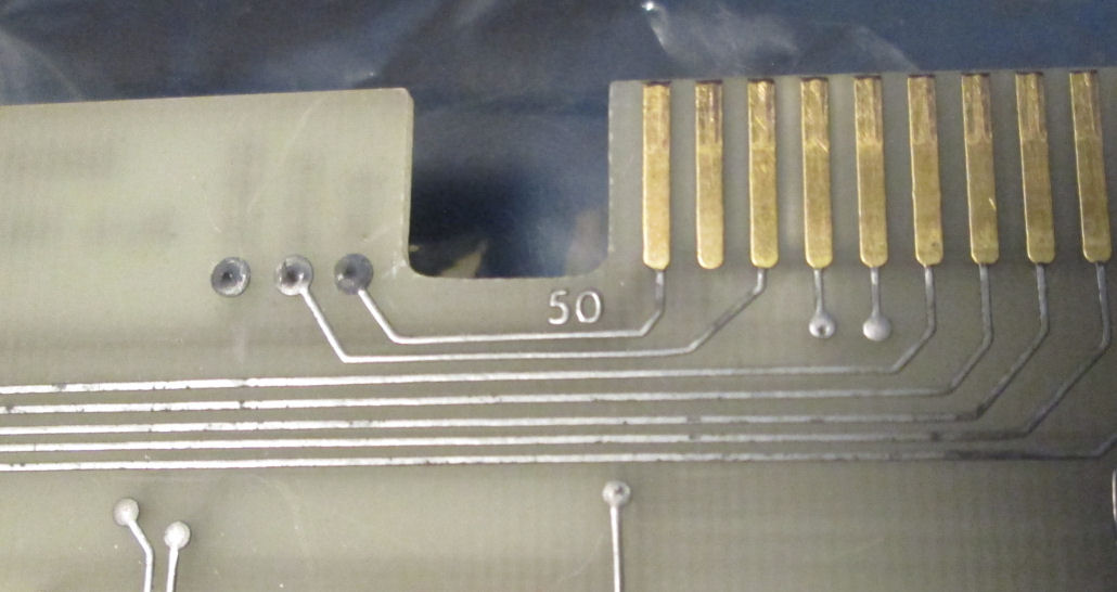
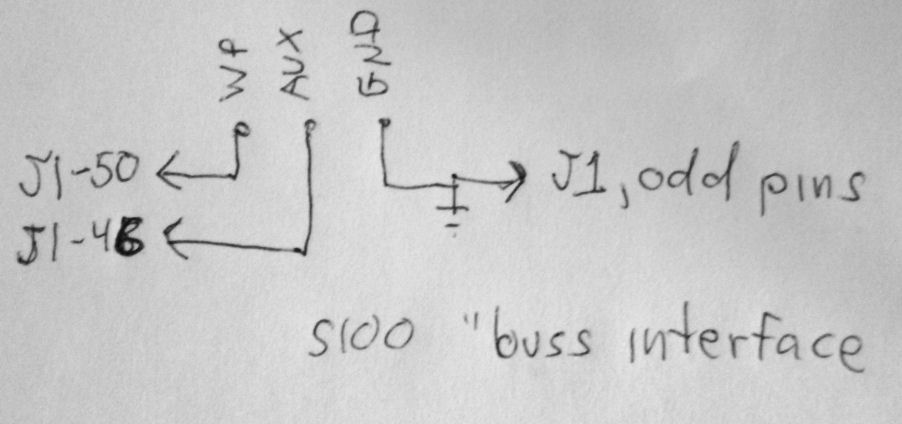
I happen to have convenient, a buss interface board, "HB 1.4". Here's an image of the cabled edge of the board where it cables to the FDC, the disk controller. YOu can see the identifying text. Also, see three jumpers marked "WP AUX GND". YOu can see that "GND" is clearly connected to PC board trace to pins 49, 47, 45, etc. Obviously: ground. Looking at the back of the board at the three jumper pins, you can see pin 50 of the connector goes to "WP"; pin 46 goes to "AUX". The schematic is trivial but here it is.
I went back to my available 3.31 FDC board, to examine pin 50 of J3, to the buss-interface board. I attempted to trace the connections. Please keep in mind: I do not know if this buss-interface card was used with this drive-controller. In any event, I traced pins 50 and pin 46.
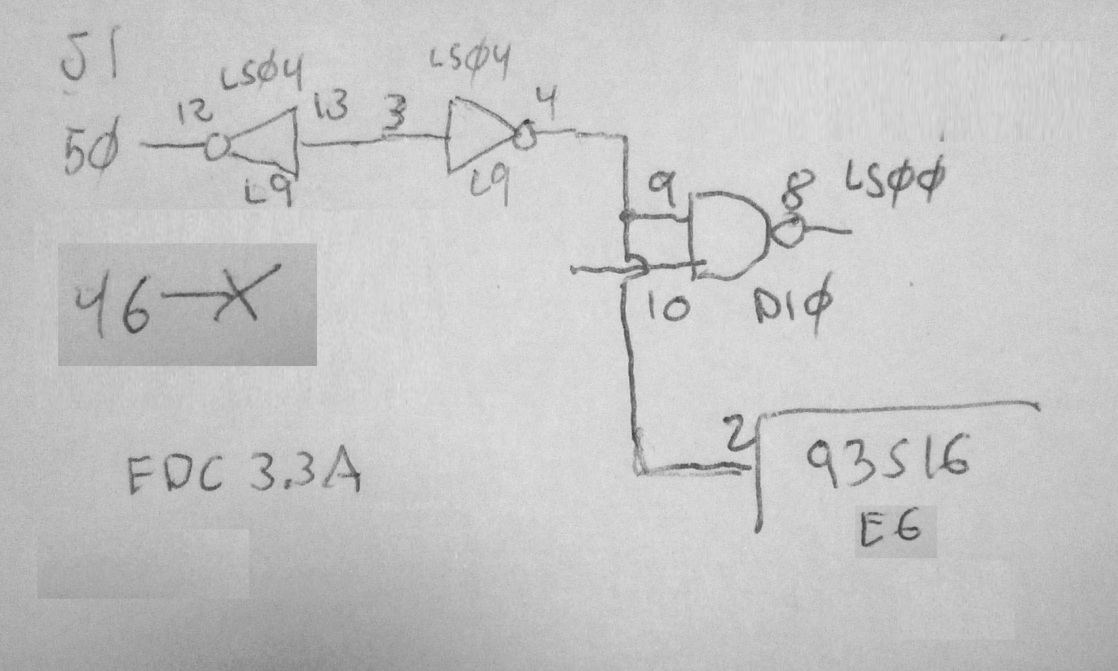
Here's my schematic of pin 50 (and 46) for the buss-to-FDC interface connector J1. First, pin 46 - AUX - goes nowhere. Second, pin 50 connects to the output of chip 74LS04, pin 12, located at L9. The input of that inverter, connects to the input of another inverter on chip L9 This makes no sense: the line at the buss-interface end is either open or grounded. You never connect a TTL output to ground! And it's pointless to have two TTL inputs connected to each other, but not to a TTL output.
Third: the chip location "L9" looks to me, like an afterthought; an added chip to the design. I conclude this is some kind of "goof", the inverter at pins 12/13, was wired in *backwards*. Or, I goofed in tracing the board. It's possible, but I checked a few times! [But keep reading...]
All that considered, I drew part of the remaining circuit. The second inverter, pins 3 and 4, is properly connected at pin 4, to two chips. One is an input of an NAND gate: pin 9 of the chip at D10, a 74LS00. The other connection, is again an input, to pin 2 of a 93S16, at location E6. The 93S16 is a reloadable counter. It's pretty busy and I did not detail its operation or trace it further. Or, trace the 2nd input at D10 pin 10, or the NAND gate output pin 8. I do see visually, that E6 has connections to E5, a 74S287 TTL PROM (256 X 4).
I went back to the Dec 1976 FDC-1 schematic, to look for a 93S16 counter, a 74S287 PROM, and to look for connections to J1 pin 50. Well. Pin 50 is not shown on the schematic; presumably it's not used. I don't see the 93S16 or a 74S287 PROM. So at this point, I don't know what to make of the function for shorting pin 50 of J1 on the FDC version 3.31 board. And, my schematic for the "HB-1.3 Bus Interface", does not show a connection to pin 50 of J1, or pin 46 either.
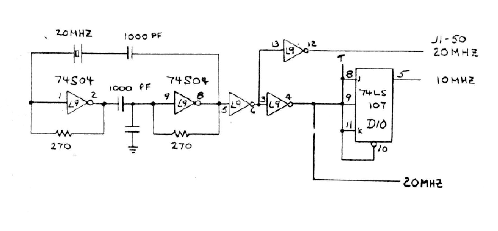
Later, I went to the "Dig_Sys_FDC3.pdf" document, and looked at another part of the FDC 3.3 schematic there. On sheet 1 of 3, there at the top of the page, there's a schematic of a 20Mhz clock circuit based on inverter 74S04 at L9. And sure enough, there's an inverter pin 13 (in) and 12 (out), which shows its output to "J1-50 20MHz". My drawn schematic is a little different, but I show it's an output from L9 pin 12. I show the inverter L9 pins 3 & 4 correctly too. What I apparently failed to find, was the additional connection to inverter L9 pins 5 and 6 - which provide the missing input to pins 13 and 3; namely the 20MHz clock signal.
Whatever the purpose is for offering a 20Mhz signal to the buss-interface card; it's nothing to do with drive "write protect".
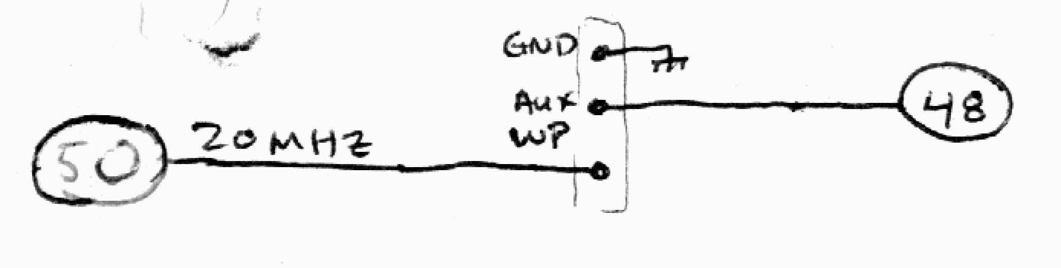
And, also a part of the "Dig_Sys_FDC3.pdf", is a copy of the HP 1.4 schematic - heavily modified by hand - which shows pin 50 and pin 48, and the three-pin jumper. It's the same schematic I drew a day prior. Regarding the "AUX" jumper to pin 48: the 3.3 FDC schmatic does not use J1 pin 48, it does not appear on the schematic.
In July 2019, Dwight Elvey commented on his use of write-gate in his DS controller. Dwight is a tech/engineer from the era who is still working on this vintage stuff. He decoded a DS controller FDC-II's microcode as discussed on my Digital Systems Web page. Here's what he said in July 2019. - Herb
"I see you've been working on your [DS floppy] controller. I was referencing your page and I thought to see if any new information had been posted. I don't recall having any particular issue with the write gate control on my setup. From what I gather, the Format was controlled by a separate ROM chip that was an extra part that one bought ( luckily my machine came with it )."
"There was a jumper on my interface card to enable formatting. I think this is different on the type 3 controller. I added a switch on the back of my IMSAI machine for this switch. During format the IMSAI's software had to provide the header and sector data, as well as doing the track stepping. The controller provided the CRC so that part was easier. Software provided an entire track of header and sector data for one DMA transfer, as I recall."
"Once formatted, writes and reads worked the same except one control bit. I don't recall anything special about DS0 and write protect but I could have missed it or ignored it. I've not look at this stuff for some time but I could go back and look at things if you need more help." - Dwight
I looked at my copy of Dwight's FDC-II documentation; and in fact the FDC-I FDC Controller Interface manual, has an update at the end for the FDC-II S-100 interface. It says "WRITEPROT (pin 50 on FDC-2) (J1-09 on FDC-1) (must be low to write on diskettes)". It also says "-AUXPROM (pin 46 on FDC-2) (J1-60 on FDC-1) (low for initialization ROMS). The DS documentation notes that "initialization ROMS" for disk formatting, are an extra-cost item. In the era, it was not unusual for floppy-controller companies to restrict the ability of end-users to format their own diskettes!
- Herb Johnson
This page and edited content is copyright Herb Johnson (c) 2019. Copyright of other contents beyond brief quotes, is held by authors of that content. Contact Herb at www.retrotechnology.com, an email address is available on that page..