![[11/04 front]](1104_panel.jpg)
This page Last updated JUne 2014. My other DEC stuff is on this linked Web page. To email me, see see my ordering Web page for my email addresses.
I acquired this PDP 11/04 and two RL01 drives in summer 2013. I've not had an opportunity to work on the system until June 2014. - Herb
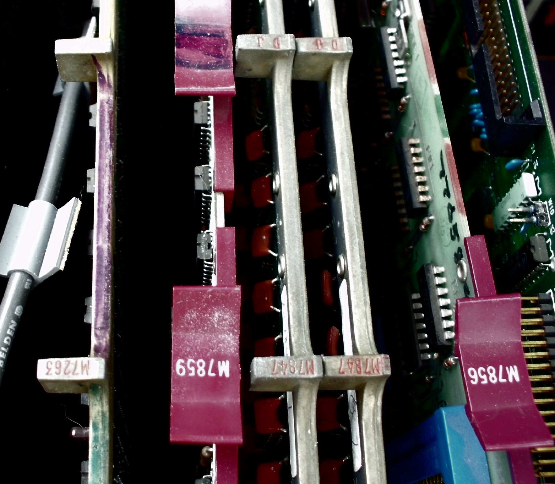
![[11/04 front]](1104_boards1.jpg)
Cards in my 11/04, front to back (right to left), are
(front console)
M7263 -      hex KD11-D 11/04 processor module
M9301YA dual / M7959 quad
   M9301 is  boot ROM and diagnostics? and terminator
   M7859 is  KY11-LB Console interface and programmers console
M7847 DJ  -  hex MS11-JP 16-Kword 18-bit RAM
M7847 DJ  -  hex MS11-JP 16-Kword 18-bit RAM
bus grant jumper board
M7856     - quad DL11-W RS-232 SLU & realtime clock option
bus grant jumper board
FD 1100I  - quad SMS brand controller board, w/white handles & three IDC (male flatcable) connectors, 50 34 34 pin
The chassis label shows the chassis as DBA11-KA.
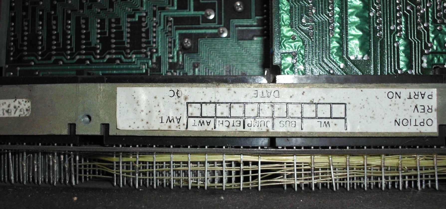
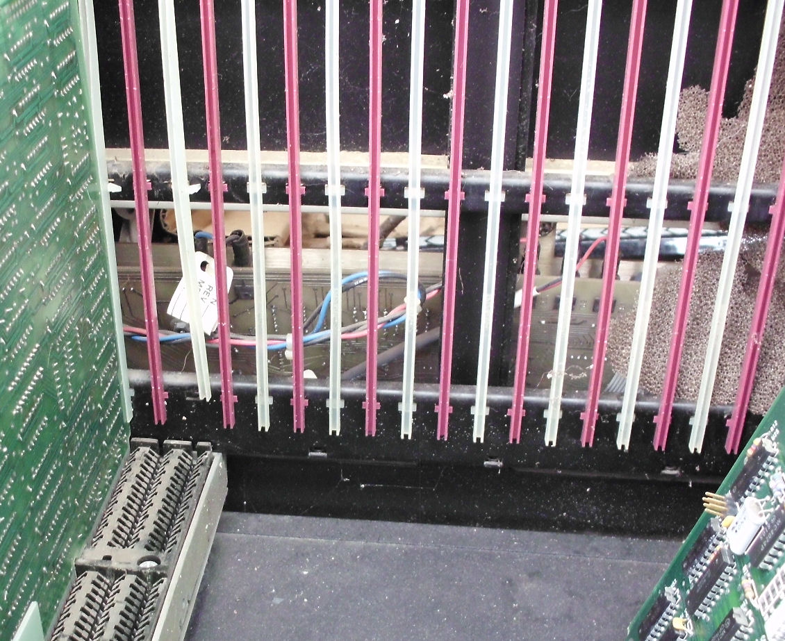
A view under the backplane looks clean enough.
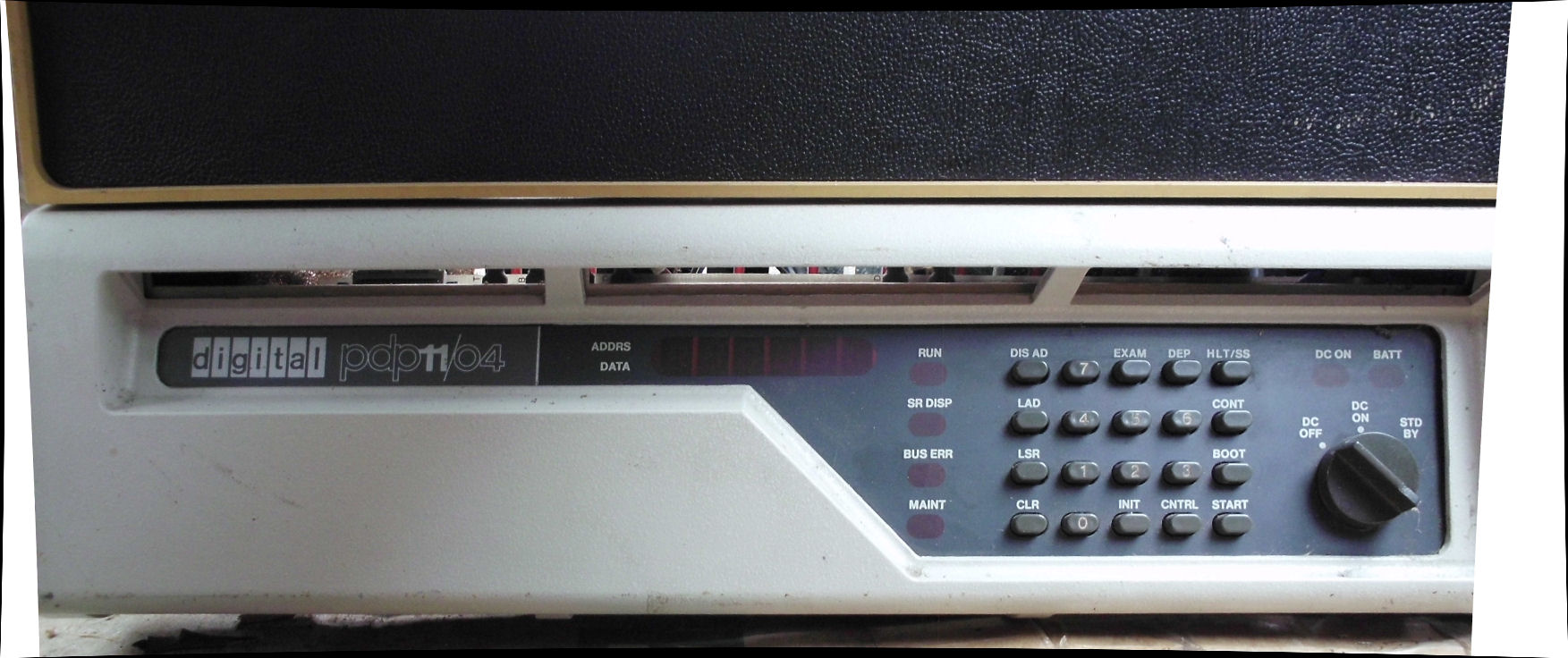
Detail photo of the front control panel. The filter behind the front panel is of course degraded.
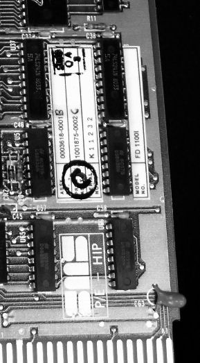
![[11/04 SMC board]](1104_sms1.jpg)
The likely Scientific Micro Systems board has badges (lables, printed stuff) such as "SMS P/E-HIP" and "model number FD 1100I" (not FD11001) "Serial number K112xx" as in this photo. Chip dates are mid-1980. Board has "fab 0003620-0001C". Three male flatcable connectors, 50 34 34 pin each.
Another PDP-11 site shows an 11/04 with the same "white handle" board and identifies it as 3rd party disk controller SMS FD1100I .
In June 2014 a Web search found on a SMS "PDP-11 HIP" schematic. Here's my analysis of the schematic. The 50-pin connector has many grounds on it in an odd pattern. The two 34-pin connectors have ground on the odd pins (mostly). J104 (34-pin upper right of board) shows similar 8X300 related lines. J101 (50-pin upper left of board) shows "address" and "instruction" lines from the 8X300 microcontroller.
J06 (34-pin upper center of board) shows 8 bits of data on pins 18-32 even, other lines have DCTRL, PROTCL, IDLE, N, XFER, ACI, SMD, RES. I conclude the center 34-pin J06 is the interface connector.
Also on bitsavers is a FD0300 brochure. The FD 0300 is a SASI to floppy controller board. The price list shows a series of SMS microcontrollers including the "FD1100 series, complete PDP-11 floppy disk controller (IBM 3740 compatible) FD1100X" where X is a digit 1 to 6 for interfacing: Orbis 76/77; Shugart 800; Pertec 400/500;
Innovex 210; Calcomp 140; CDC 9404. But the SMS FD1100 flyer on bitsavers, is for a hex-width card much larger than my quad-width card.
My guess, is that the FD1100I is a smaller version of that floppy controller. But floppy controllers don't have 8-bit data connections, they are serial. Possibly this is a SASI controller board? I'll have to look at SASI documents.
I'm told it was powered up in 2013. I've not had an opportunity to work on the system as of June 2014. - Herb
Copyright © 2014 Herb Johnson