This note is superceeded by Rev D of the Membership Card as of July 2012. Rev D and later revisions include jumper support for stacking two CPU cards. Here's the link for stacking two later-revision CPU cards.. Meanwhile, this note may be useful for Rev D, and a link to an earlier note for Rev C may be informative. - Herb Johnson, May 2022
This note was produced Jan 6 2012 from discussion from Lee Hart about some responses on cosmacelf. I edited it to make it a coherent document. In April 2012, I've reedited and added some specific "mods", with more notes from designer Lee Hart. Support for the COSMAC 1802 Membership Card can be found on the linked Web page. Preliminary material added April 1 2012. 2012 (c) Herb Johnson
Lee Hart, early 2012: I worked long and hard on the Membership Card, trying to get both RAM and ROM onto it. I just couldn't find a way (without leaving something else off, or using surface mount, or some exotic chips, etc.)
So, I contented myself with a single bytewide RAM socket, and a little supercapacitor to maintain memory. This works fine when it's easy to download programs into RAM. There are also some nonvolatile RAMs I wanted to play with (but haven't yet).
[But after some discussions about expanding the Membership Card,] it just dawned on me that we could take *TWO* Membership Card CPU boards, and stack them! Pull the 1802 CPU chip from the bottom board's CPU socket. Use a wirewrap socket for the 1802 on the top board, and plug the lower boards's 1802 socket into the end of the upper board's wirewrap socket.
Stack the boards far enough apart so the 30-pin I/O header on the bottom board doesn't reach the upper board. This header has all the pins for a second available I/O port, and duplicates of all the power ground and other I/O and control signals.
To keep the boards from "fighting" and to share resources:
  - Disable the clock (U4D) on one of the boards.
    (so the two clocks won't fight each other).
  - Change the I/O port address of one of the boards.
    (U4A inputs move from N2 to N1, for example).
  - Put a RAM on one board, and a ROM on the other.
    (can have something like ElfOS perhaps).
  - Replace Q1 with a pair of diodes on one board.
    (so its memory is at 8000-FFFF instead of 0000-7FFF).
A Front Panel board can still be plugged onto the top board, and will work normally.
This seems like a neat "hack". It doubles the memory, doubles the I/O, and doesn't require any new boards to be designed. Having both RAM and ROM means programs can be pre-loaded. :-)
Last edit Apr 1 2012 Herb Johnson.
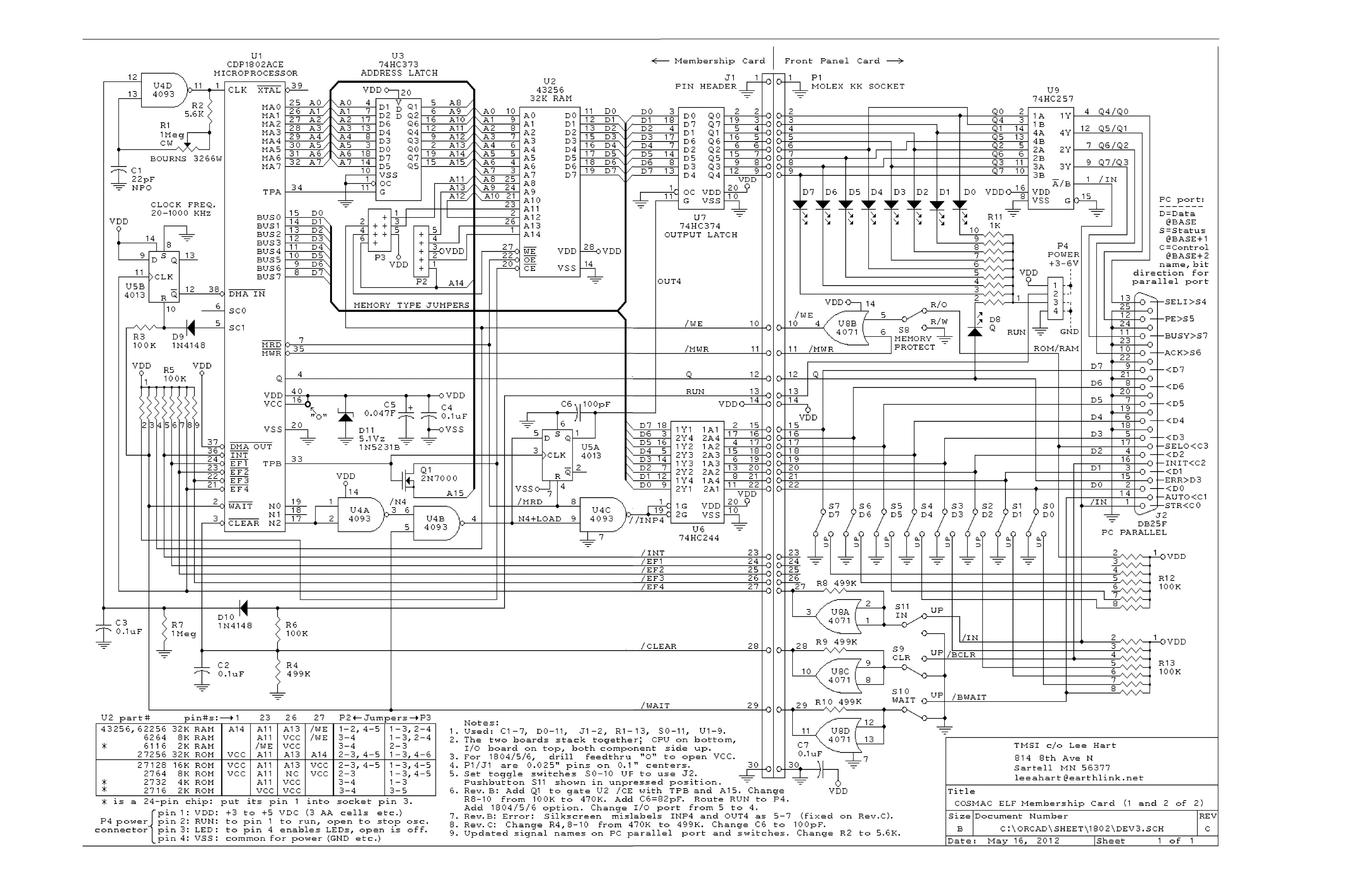
Refer to the Rev C Membership Card schematic for parts and pins. The board on top will hold the CPU chip and be called the "processor board"; its wirewrap socket plugs into the bottom CPU board which will be called the "driven board". The driven board will have a ROM, the processor board will have a RAM.
Bring out N0, N1: Disconnect /MWR from header pin 11; and /WE from header pin 10. Short /MWR to /WE. The ROM is on this board so write control is unnecessary. Connect header pin 10 to CPU pin 19 to access N0; connect header pin 11 to CPU pin 18 to access N1.
ROM address in upper memory: location depends on size of RAM and ROM. Details may be tricky. But as 1802 uses page 0 space for reset, interrupt, and special addressing, RAM should be in low memory.
I/O adr 5: Break U4A connection between pins 1 and 2. Connect pin not connected to CPU pin 17 (N2), to CPU pin 19 (N0). Now U4A decodes I/O address 5 on this board. While this could be done on either CPU board, the front panel is programmatically accessable by N4 instructions; the front panel would be or is connected to the CPU board on top. So re-addressing I/O makes more sense on the "driven" CPU board on the bottom.
disable RUN: Disconnect U4D pin 11 from CPU socket pin 1 (CLK). Remove R2 and R1 potentiometer, and C1 either shorted or removed. U4D NAND gate is available for other uses. RUN line from header pin 13 available as external input. R6 must be removed or disconnected from /CLEAR line, possibly used as pullup to +5. R7 possibly changed from 1M as pull-down, C3 removed or not, D10 retained or shorted.
possible negative voltage pump from U4D: steal CLK from pin 1, to drive gate U4D, to create negative charge pump for negative voltage source for serial interface. Component space formerly used for RUN (C3, R7, R6, D10) may be useful.
disable DMA F/F: Diconnect CPU socket pin 38 (/DMA in) from U5B pin 12. F/F is reset by SC1 through D9, R3; or by /WAIT through R3 and /WAIT line from header pin 29. It's clocked by /EF4. This flip flop could be rewired for other uses, and header pin 29 available for other uses, such as a 1-bit latch, or interrupt latch.
disable power control: Remove D11, C5, C4. These are redundant. If 1804 in use, drill out shorting hold "O" which shorts CPU socket pins 40 and 16, it's also redundant.
disable WAIT, use for IN5 enable Disconnect CPU socket pin 2 (/WAIT) as redundant. Header pin 29 (/WAIT) can be used to gate INP5 when IN5 instruction active. (U6 is logic buffer, not a "latch".)
disable CLEAR: Disconnect CPU socket pin 3 (/CLEAR) as redundant. Header pin 28 (/CLEAR) is available for other use. Components C2, R4, R6 not needed or can be used with the line for other purposes.
possible use of SC0: Header lines as available could be connected to CPU socket pin 6 (SC0) which is otherwise not accessable.
RAM address in lower memory: Details of the ROM addressing may be tricky. But as 1802 uses page 0 space for reset, interrupt, and special addressing, RAM should be in low memory.
Access to ROM in upper memory: ROM will be on the "top" board as a matter of convenience to change ROMs. Challenge is to "jump" to ROM on start. One method is to simply toggle in a jump address in RAM location 0 and execute. Another method is to flip ROM and RAM addresses on reset, have ROM code on reset flip ROM and RAM to "running" address. Another method is to force a JMP on CPU at reset, or force NOPs on CPU from reset until ROM is enabled.
This page and edited content is copyright Herb Johnson (c) 2022. Contact Herb at www.retrotechnology.com, an email address is available on that page..