![[BASYS PROM pgmr]](basys_prom539.JPG)
Last updated Dec 26 2017. Edited by Herb Johnson, (c) Herb Johnson, except for content (C) Lee Hart 1982. Contact Herb at www.retrotechnology.com, an email address is on that page.
Lee Hart developed the BASYS 1802 microcomputer in the late 1970's. Check the linked Web page for details. Since year 2010, he revisited the 1802 and offers the 1802 Membership Card kit.
Late October 2017, Lee Hart sent me some BASYS documents, saying "I ran across some old notes [from 1982] on an 1802 BASYS EPROM programmers. I made copies and mailed them to you." I scanned and reviewed them. Lee followed up to say: " We built several programmers, for different EPROMs. The notes are a scatter-shot of what I had." I noticed one note was different from the rest; it's another kind of PROM programmer. The rest show a flexible design to program multiple kinds of erasable PROMs. - Herb
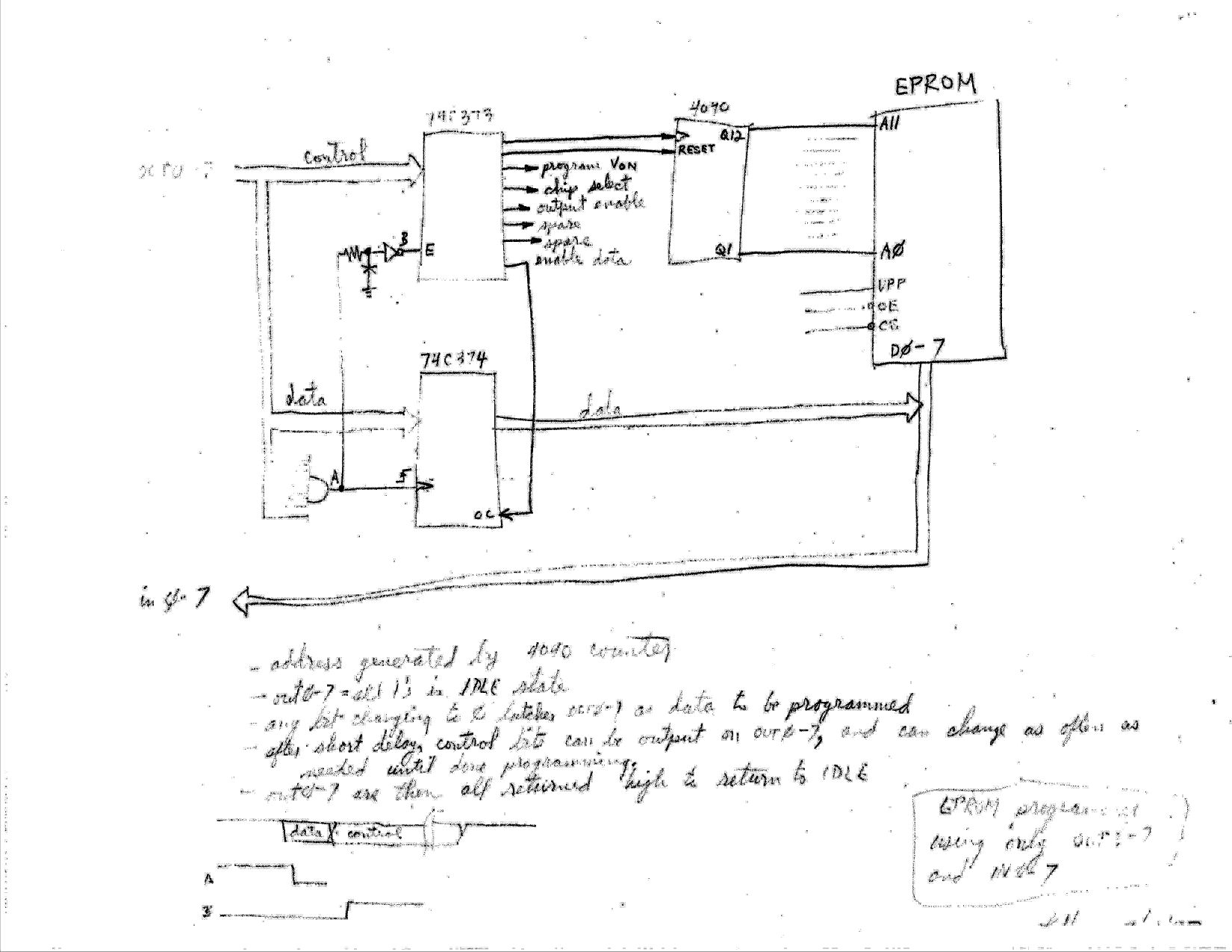
initial general concept sketch A 74C373 for control and to clock the 4040 CMOS counter; and a 74C374 for data. 1802 IN and OUT are put to use.
The address is generated by the 4040 counter, which needs a clock and a reset. Other control outputs are for the programming pulse, chip select, output enable, and data enable. The data is controlled by the 74C374 as a latch for output; input data goes back to the 1802.
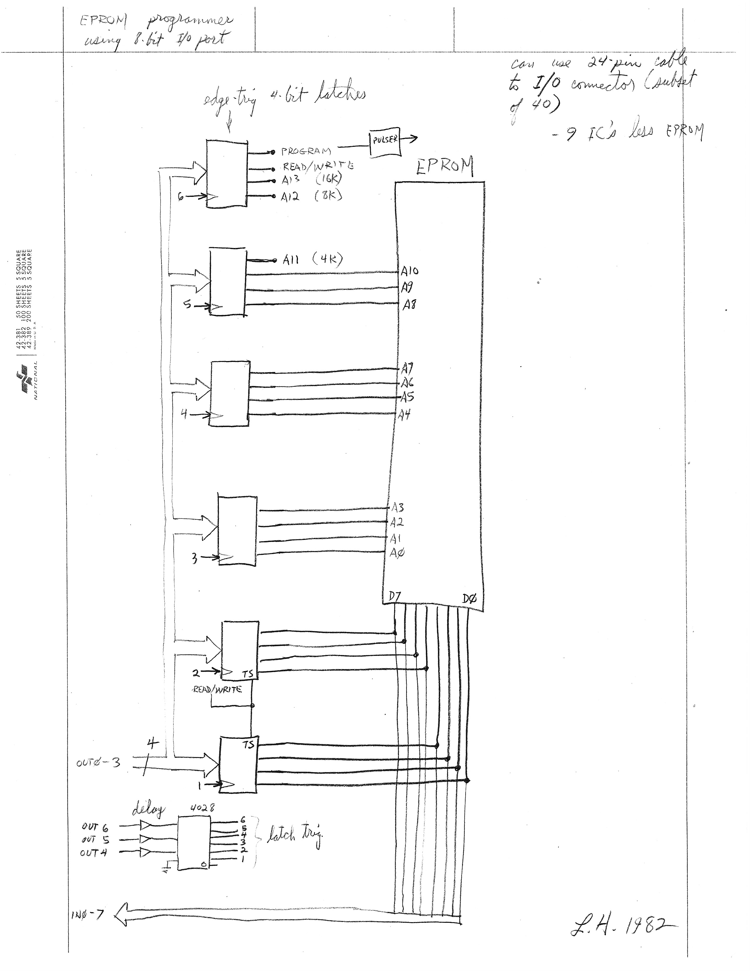
dated 1982. detail of latching address
8/18/82, schematic detail of programming voltage regulator, logic to address control signals, jumper scheme to set up EPROM selection.
Two 74C374's were used. A 74LS74 provides a pair of controlling flip-flops. Control of the programming pulse is established by a set of jumpers for connecting to the problem PROM pins.The programming voltage is likely adjusted per PROM type. The PROMS are 2716, 2732, 68764. Pulse width is a function of 1802 programming. Vcc to the PROM is also controlled by the 1802. Note the 74LS30, an 8-input NAND gate; OUT FF generates a rising edge to latch data to the EPROM.
To use:
1) write out 1's to OUT 3 port
2) write DATA to program to OUT 3
3) immmediately write control byte to OUT3 (can't be all 1's)
4) write all 1's to end cycle (data to control latches to retain contents)
5) repeat for each change in any data or control byte.
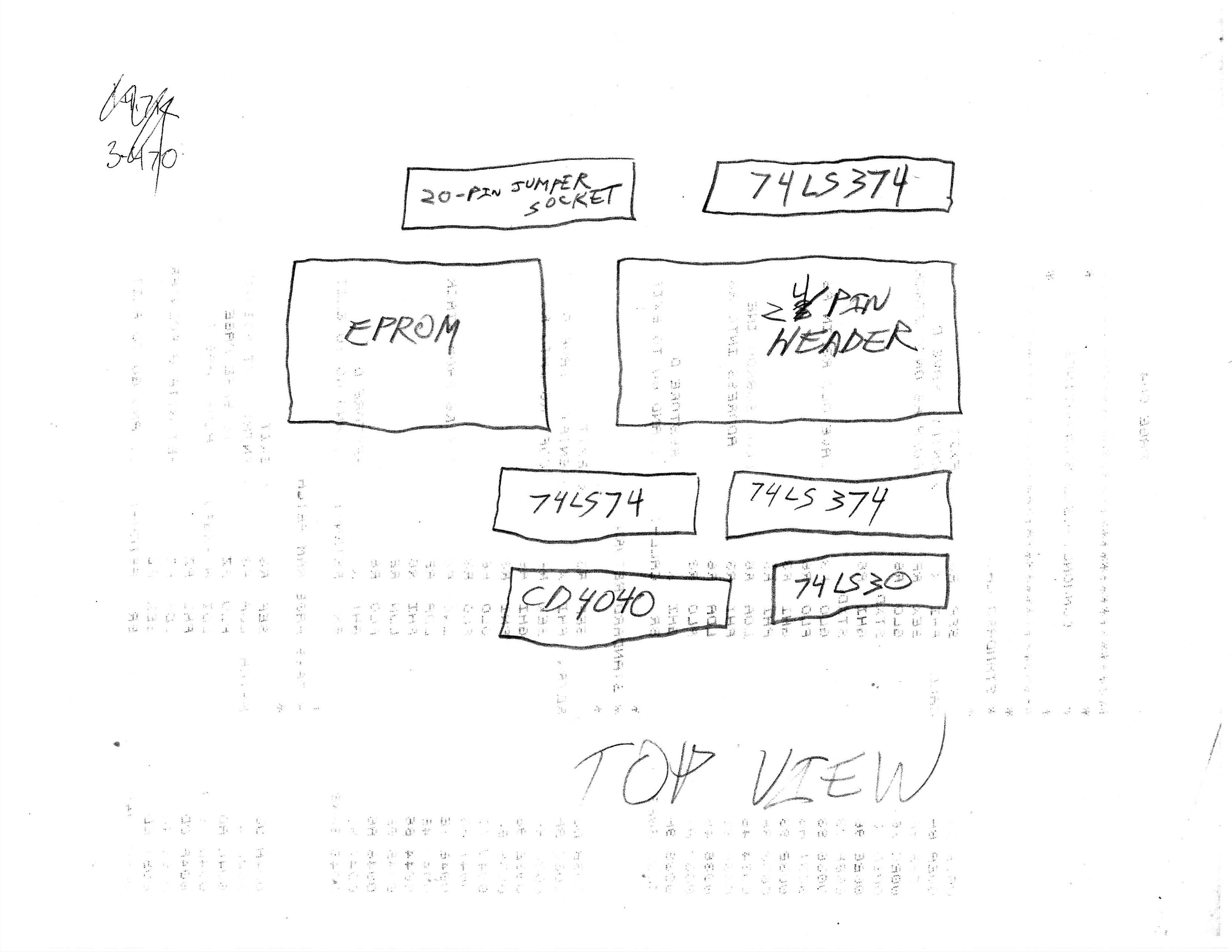
top view of chip and header layout
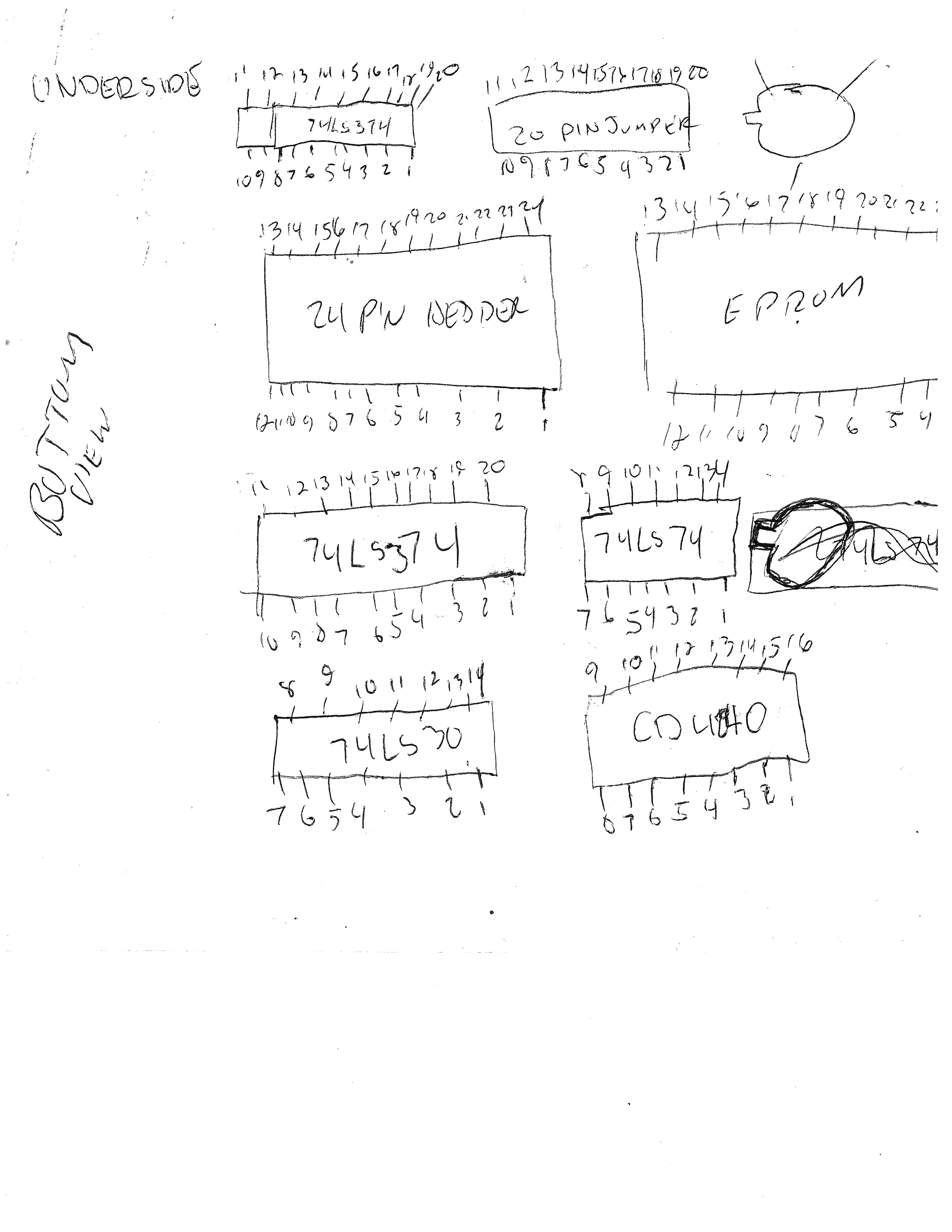
wiring side of chip and header layout
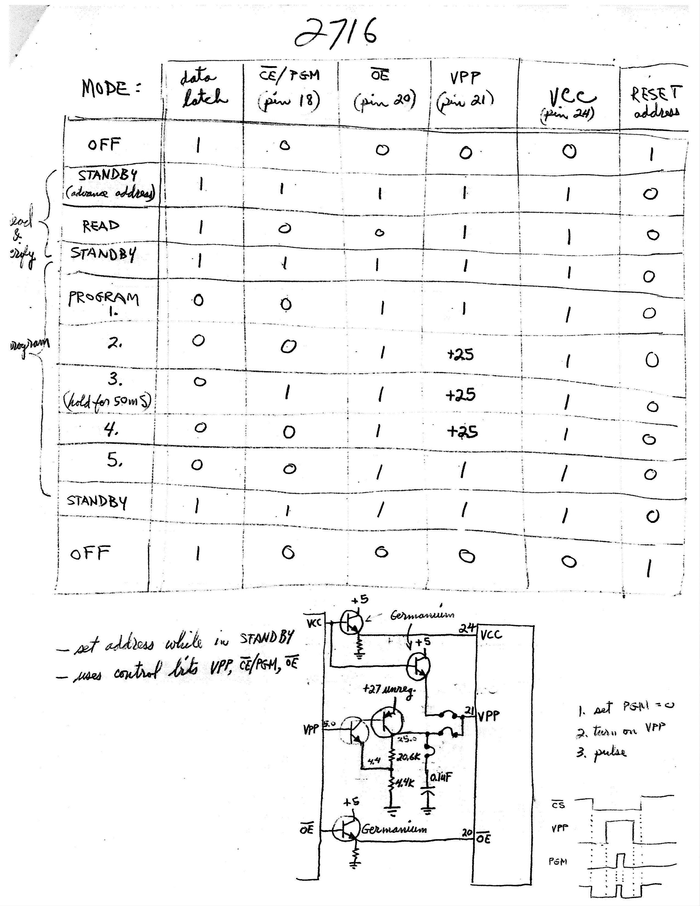
logic diagram, prog. voltage setup, 2716
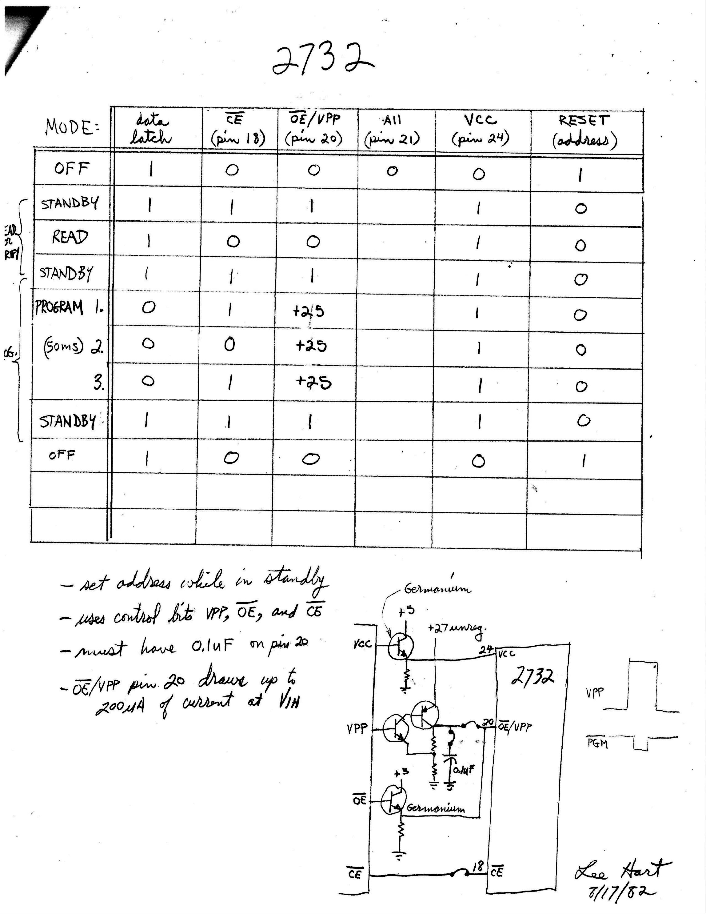
8/17/82, logic diagram, prog. voltage setup, 2732
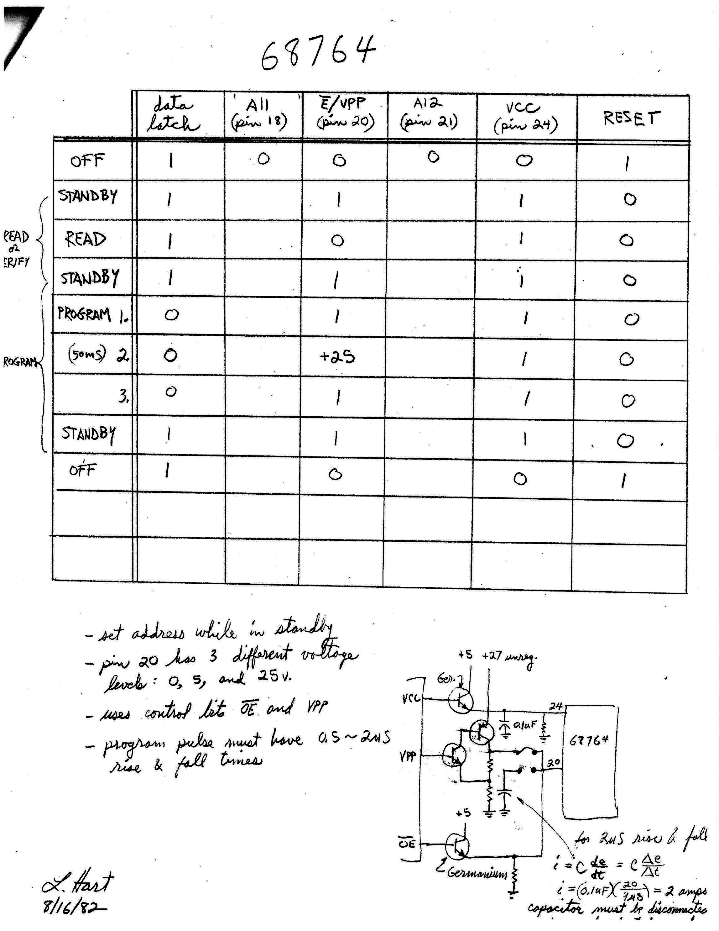
8/16/82, logic diagram, prog. voltage setup, 68764
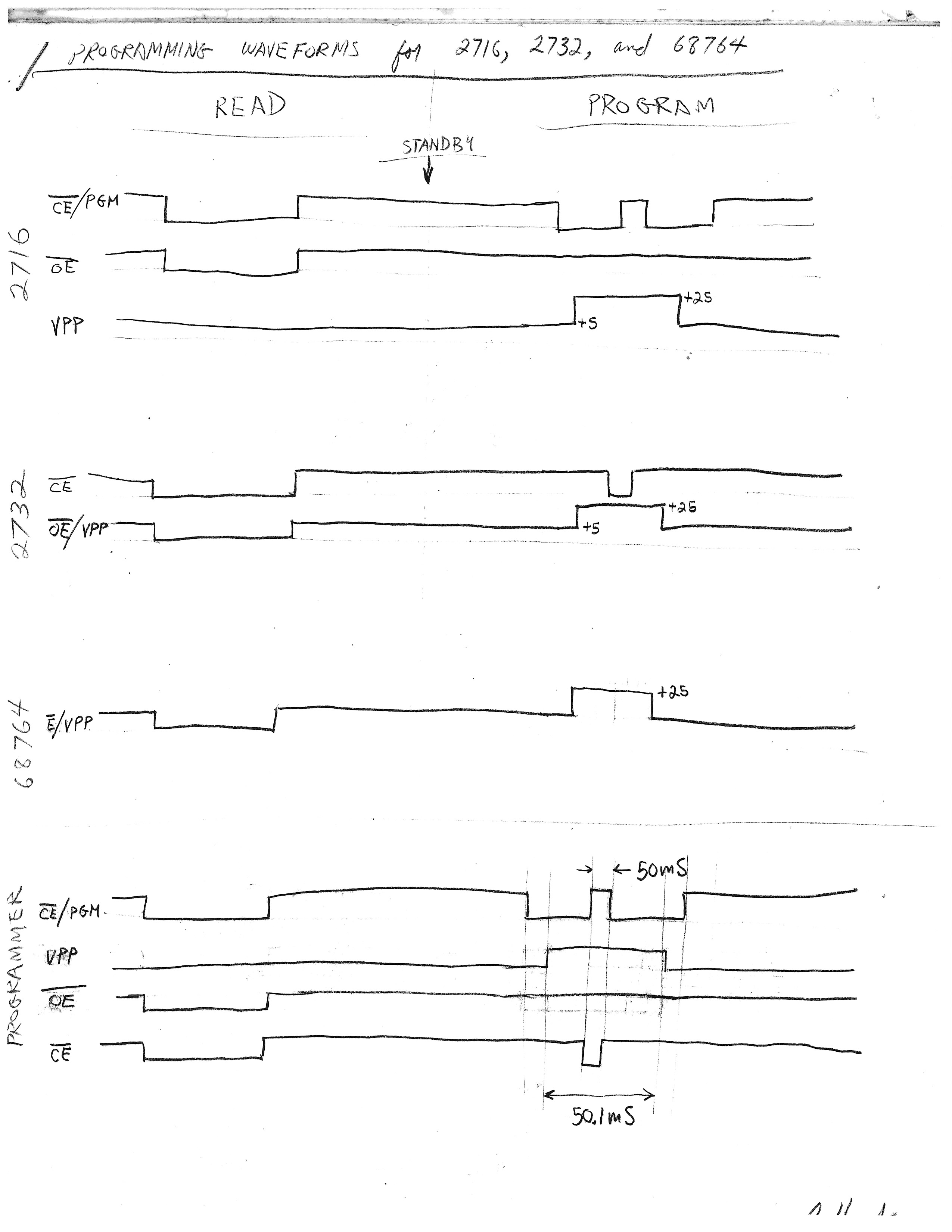
programming waveforms 2716, 2732, 68764
![[BASYS PROM pgmr]](basys_prom547.JPG)
Herb: One document looks different from the rest. It's a well-drawn PC board layout. 44 pin board. Two very large caps, four IC's near the edge connector, what looks like a heatsinked transistor. There's a parts list, six IC's 6 transistors, caps and resistors. What is this?
Lee: It might be for the Intersil 6654/6658. These were the first CMOS EPROMs; 512 bytes and 1024 bytes respectively. I used them in BASYS boards, and so needed a programmer for them. They took a LOT of power to program! The 6654 needs +40v, and the 6658 needs -30v, each at up to 100ma! So you needed a substantial programming power source.
This page and edited content is copyright Herb Johnson (c) 2017, execept content written by Lee Hart. Contact Herb at www.retrotechnology.com, an email address is available on that page..