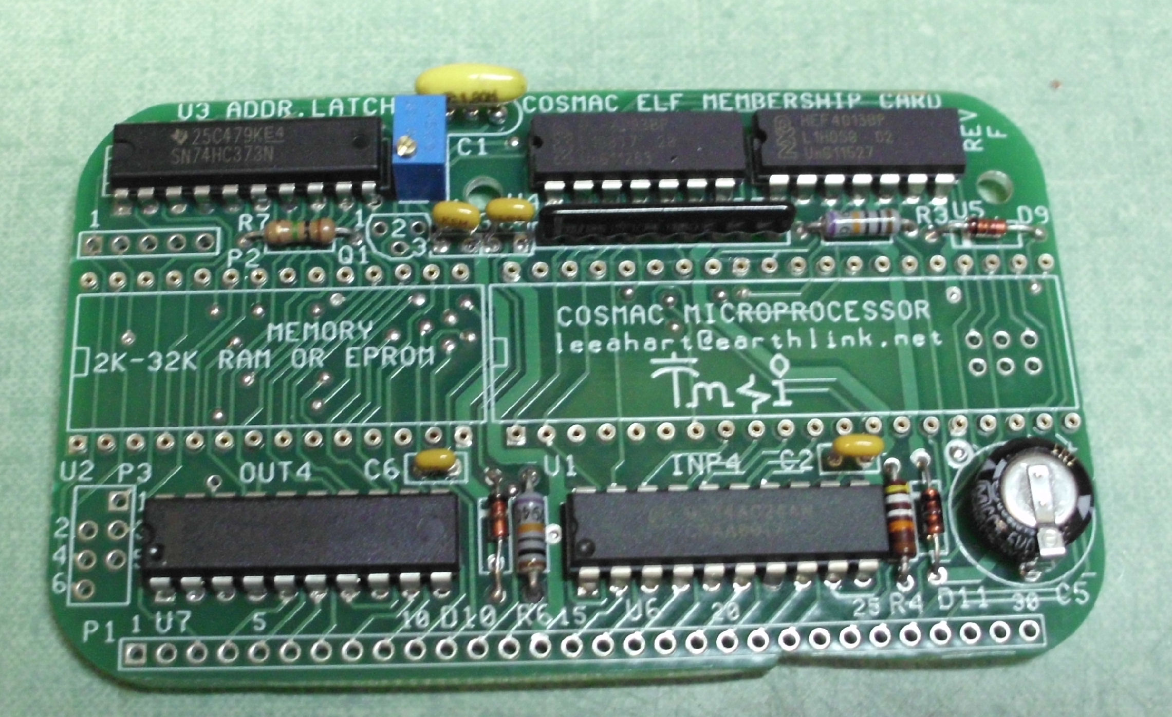
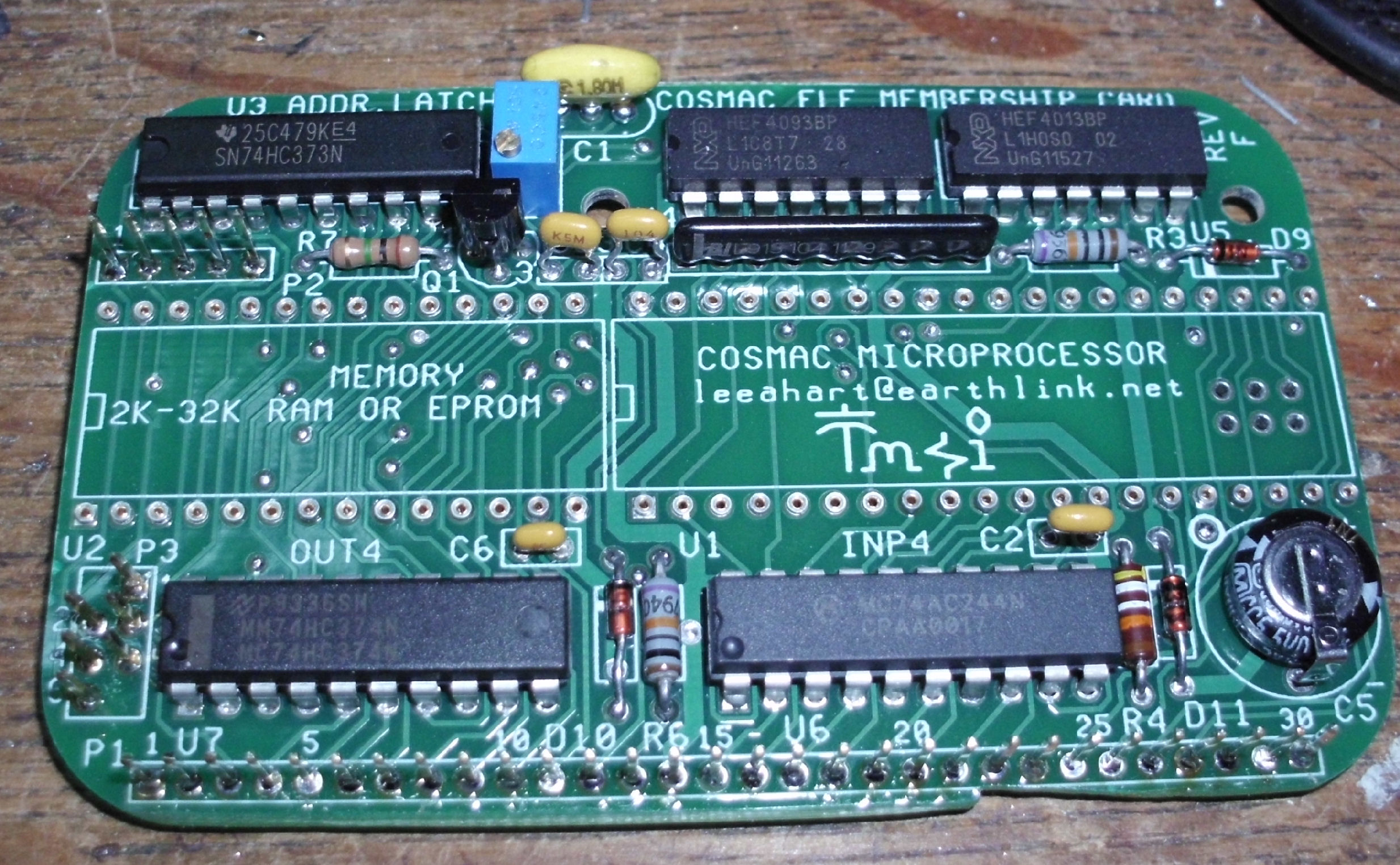
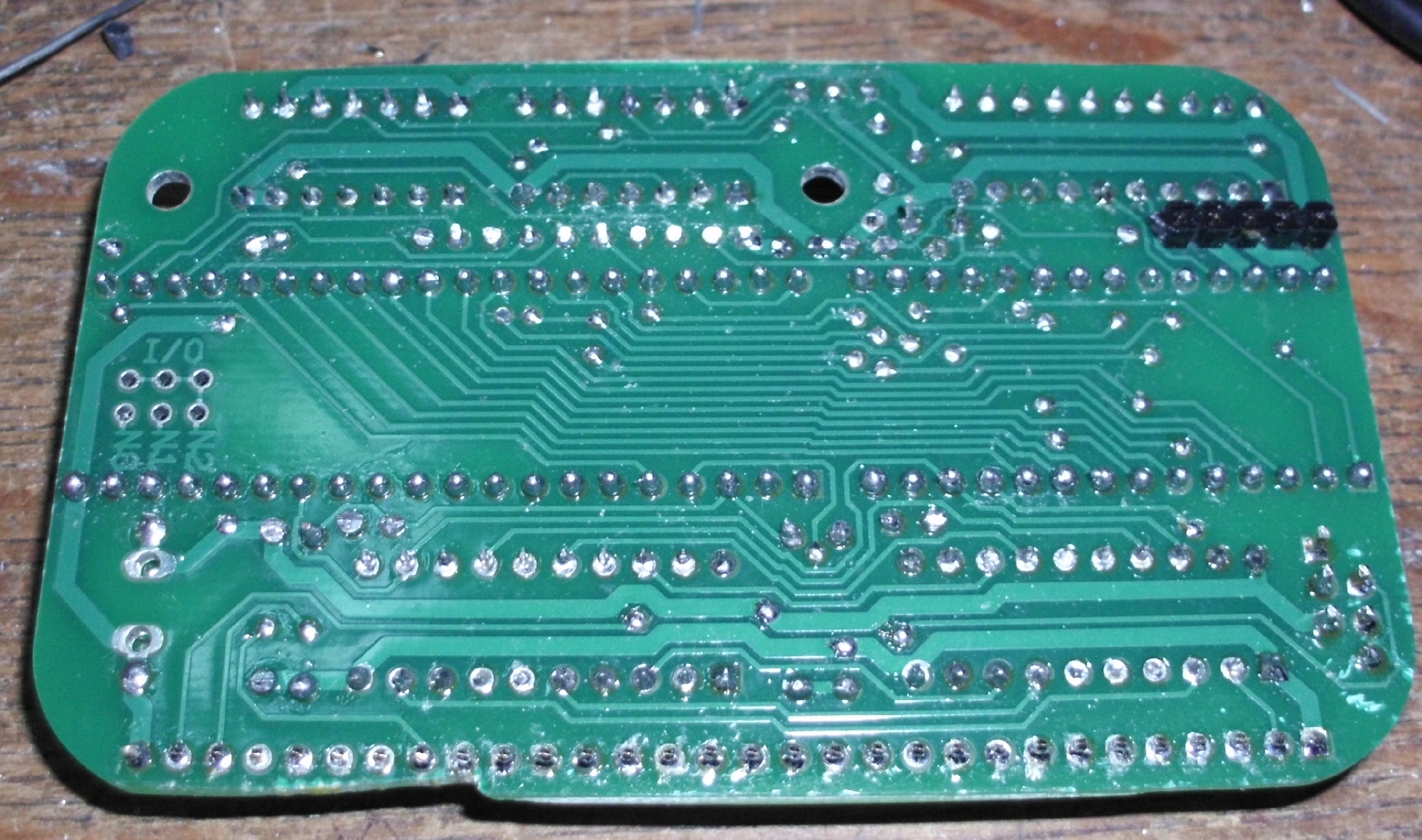
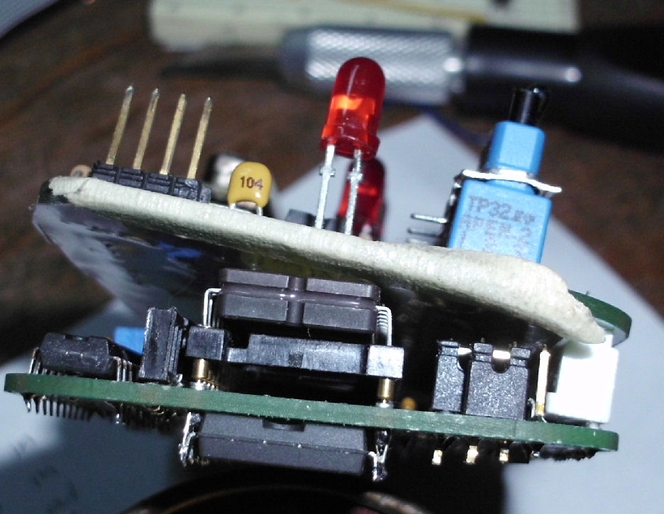
![[rev F 1802 M/S Card]](build/cpu_power.jpg)
Last Updated May 30 2016. Edited by Herb Johnson, (c) Herb Johnson, except for content written by others. homepage for 1802 ELF Membership Card.
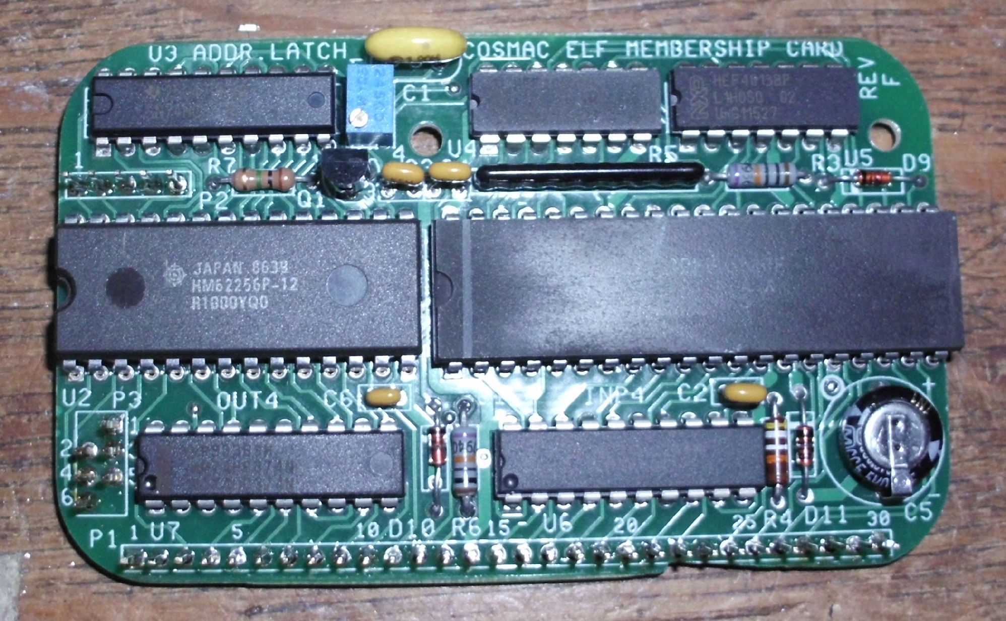
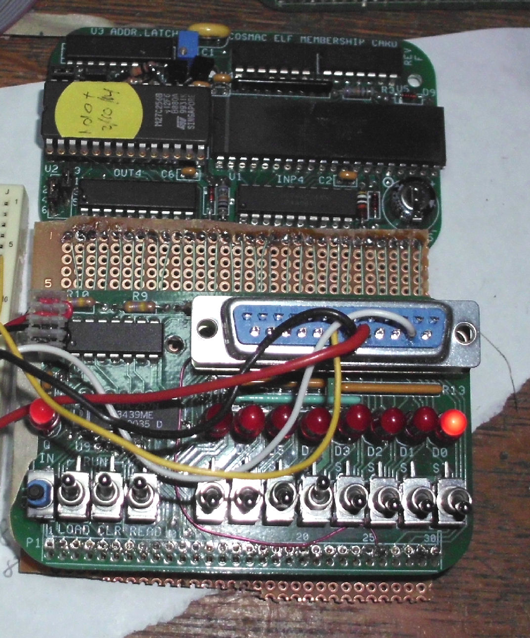
In January 2014, I built a rev F version of the 1802 Membership Card, as a show-and-tell for this Web page. The results provide some photos and comments about assembling any 1802 Membership Card. I also made modifications, and added a ROM monitor and serial interface. I built a simple board extender between the M/S cards. These mods may be of interest to owners of Revision F or earlier M/S cards; and they may be informative about building or modifying later revisions.
Also I debugged the IDIOT ROM monitor code and baud rates for the first time for the M/S card - I moved that work to another Web page in 2016.
Subesequent versions of the 1802 Membership Card support both ROM and RAM, include a serial interface, have improved address circuits. Go to the Home page of the 1802 Membership Card to access the support page for the version of interest to you.
Assembly from boards and parts
Stacking ROM and RAM
external serial interface (several circuits)
extender card PC board
Notes on debugging IDIOT code, serial interface, baud rate issues
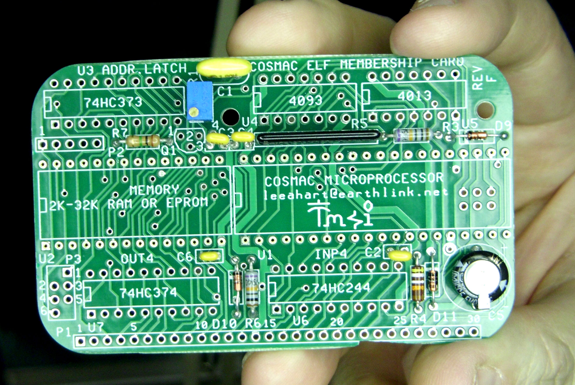
The Revision F supported either a .6-inch wide ROM or a .6-inch wide RAM: I put the RAM under the CPU board, to make room for a ROM atop the CPU board. Also, I built an external serial interface, suggested by Lee Hart. It eventually used the negative voltage from the "terminal side" of the serial line to create a negative supply for the Membership Card serial transmit. I modified a circuit which selects ROM or RAM - a mod that was put into Revision G. These all worked, with various degrees of difficulty.
I assembled and tested and debugged the IDIOT ROM monitor (inspired by RCA's UT4 monitor). You can consider those notes separately from the assembly and ROM/RAM modifications on this Web page. IDIOT was originally used on another 1802 card, the "BASYS board", and the source code needed some additions based on other BASYS software (Tiny BASIC). A useful and correct baud rate, required the M/S card to run at full speed; both a 1.77Mhz and a 2.0Mhz ceramic resonator were tested. These notes may be informative, if you are having trouble running IDIOT or some other ROM monitor on the M/S card.
The 1802 Membership Card is a very open and simple platform for the 1802 microprocessor, much like the ELF was decades ago. Work like this has contributed to the evolution of the 1802 M/S Card, and to the variety of ways owners have adapted and assembled the card. - Herb Johnson, May 2016.
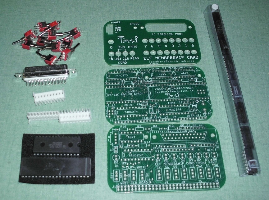
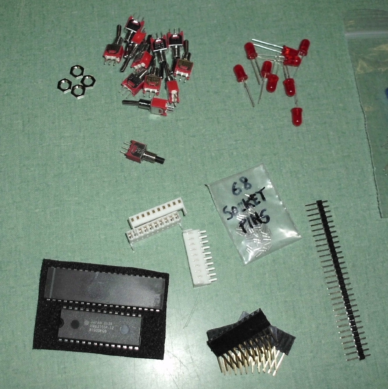
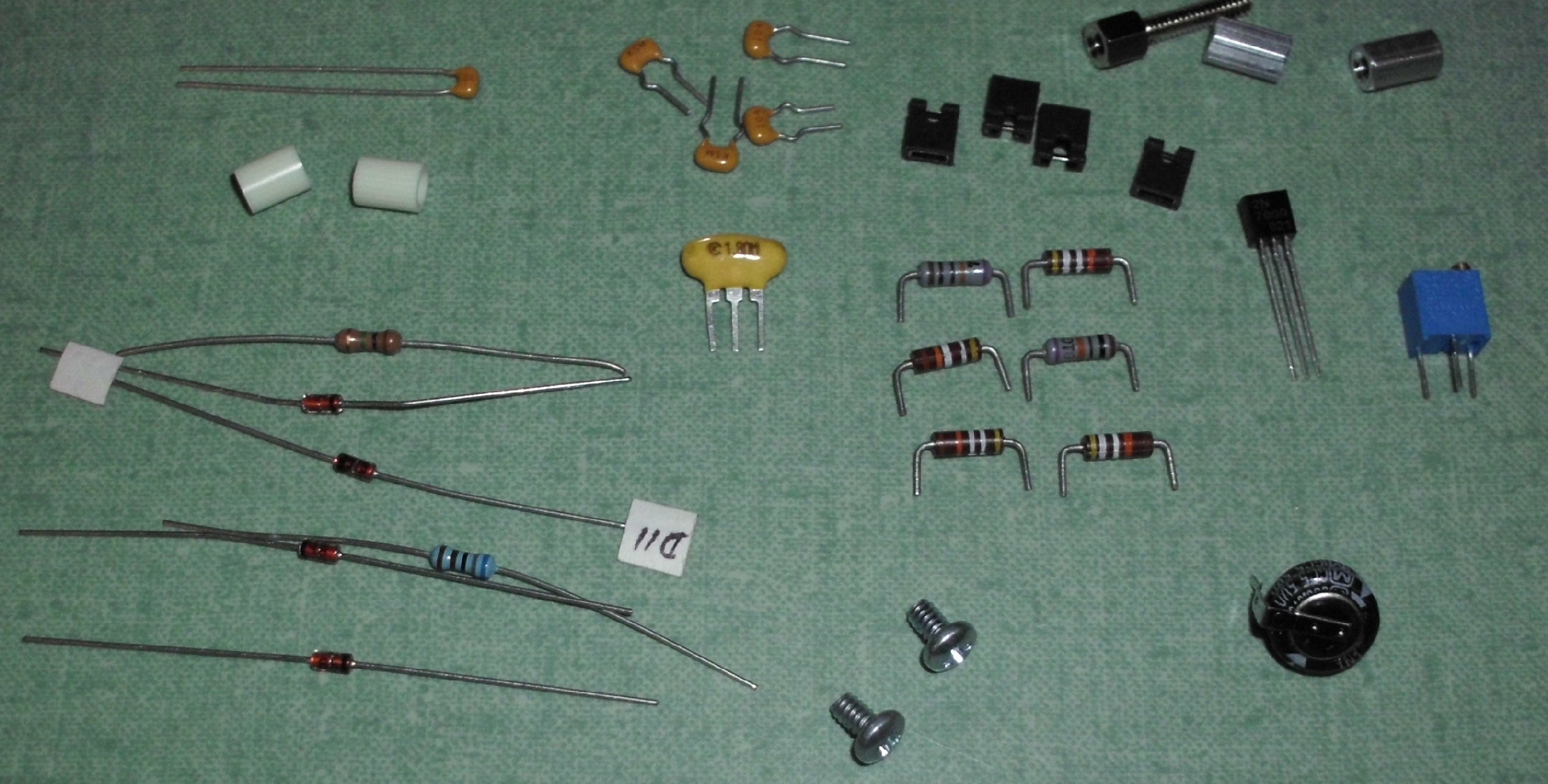
![[kit]](build/kit.jpg) kit of parts
kit of parts
boards and ICs
toggle switches, strips
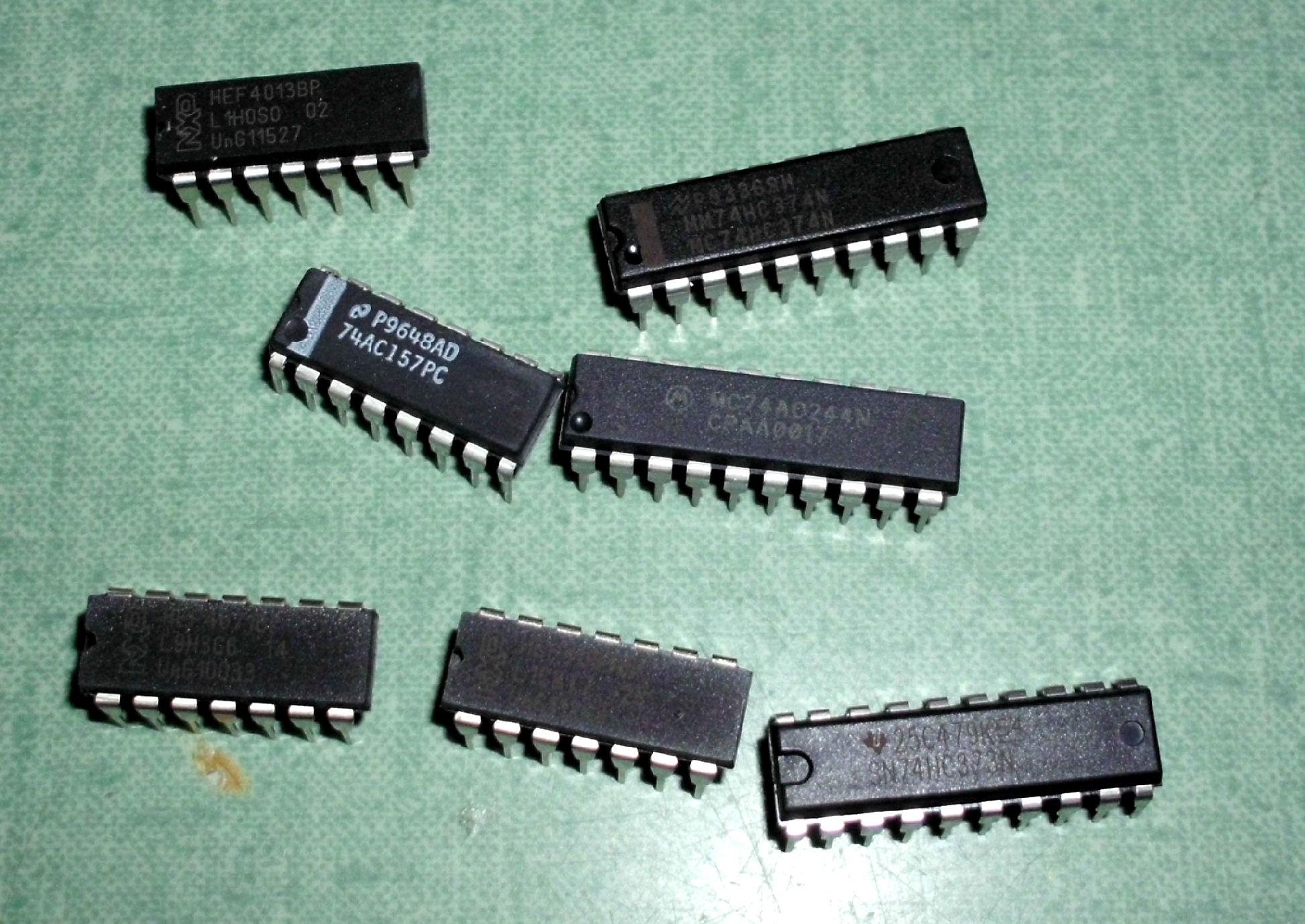
small ICs
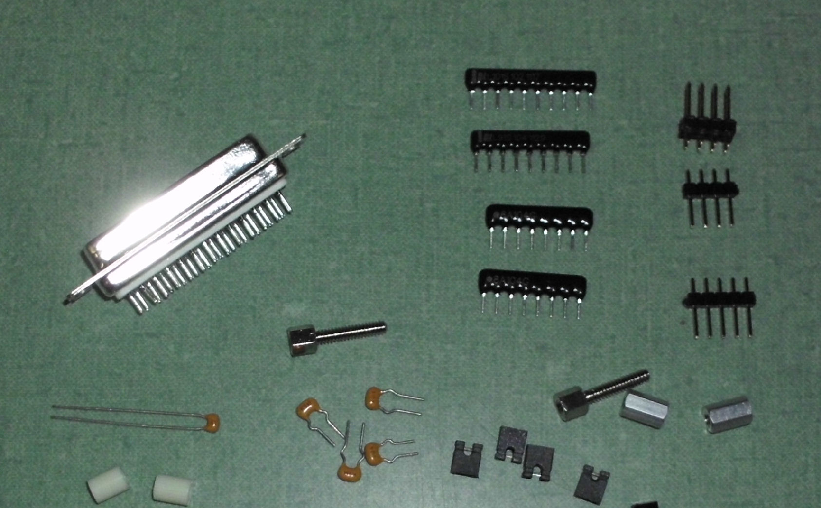
SIP resistors, capacitors
resistors and caps
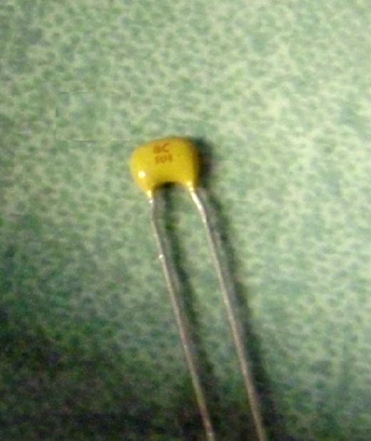
small 10**4 pF cap
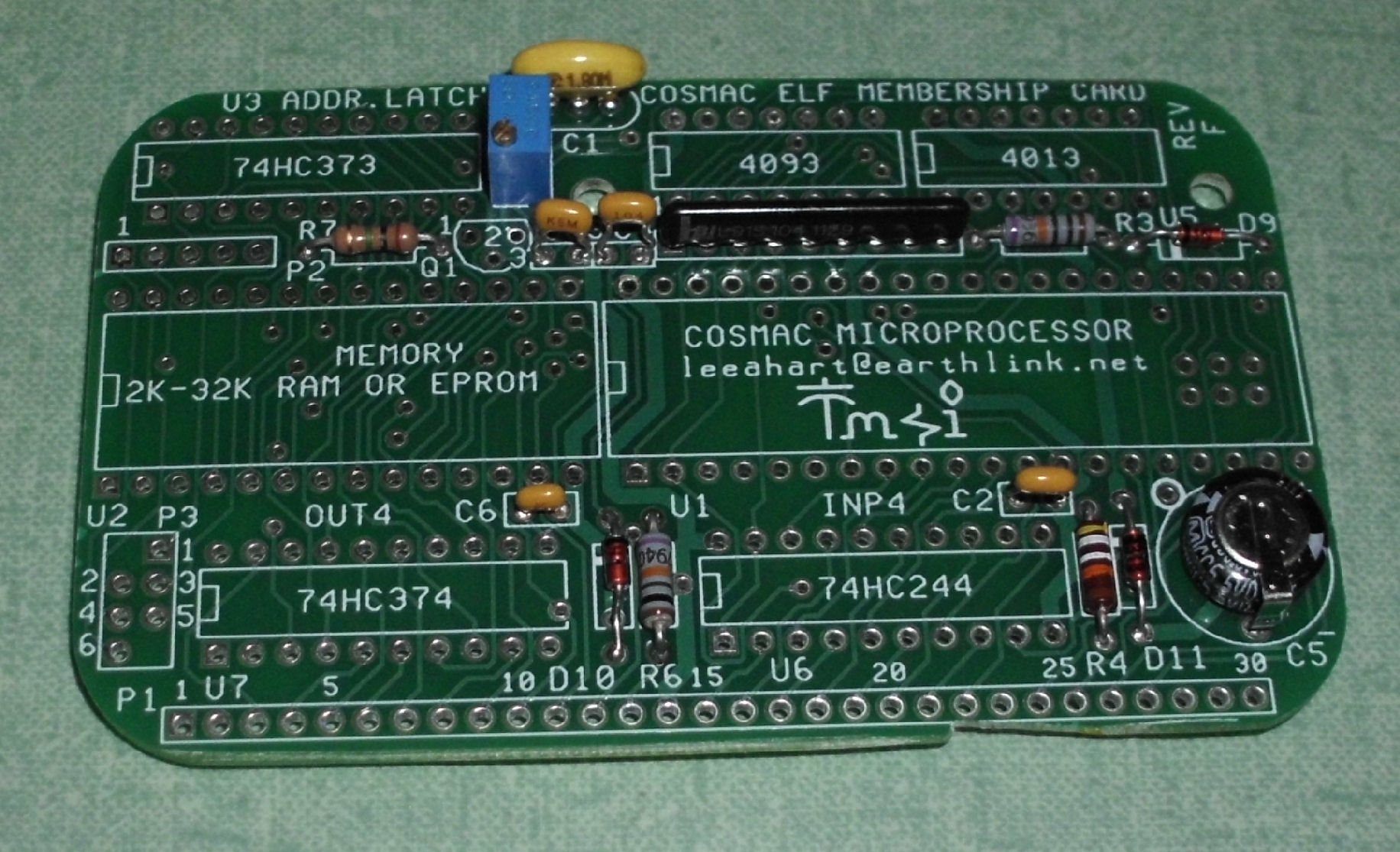
![[boards]](build/caps_board.jpg) CPU board with caps installed
CPU board with caps installed
CPU board with caps & resistors installed
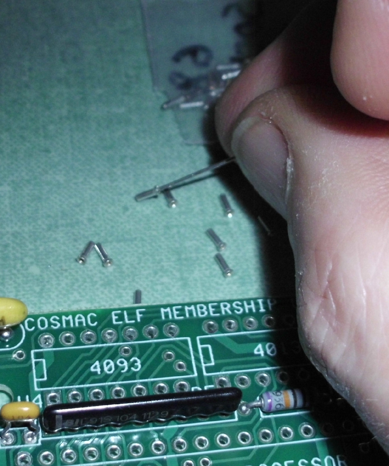
![[kit]](build/icpins_4.jpg) IC pins, individual, pick up with lead
IC pins, individual, pick up with lead
IC pins, insert one in board
IC pins, lead holds pin for soldering
CPU board with IC pins, top
CPU board with IC pins, bottom
![[kit]](build/topins1.jpg) CPU board with IC pins, Rs, Cs, top
CPU board with IC pins, Rs, Cs, top
CPU board with IC pins, Rs, Cs, bottom
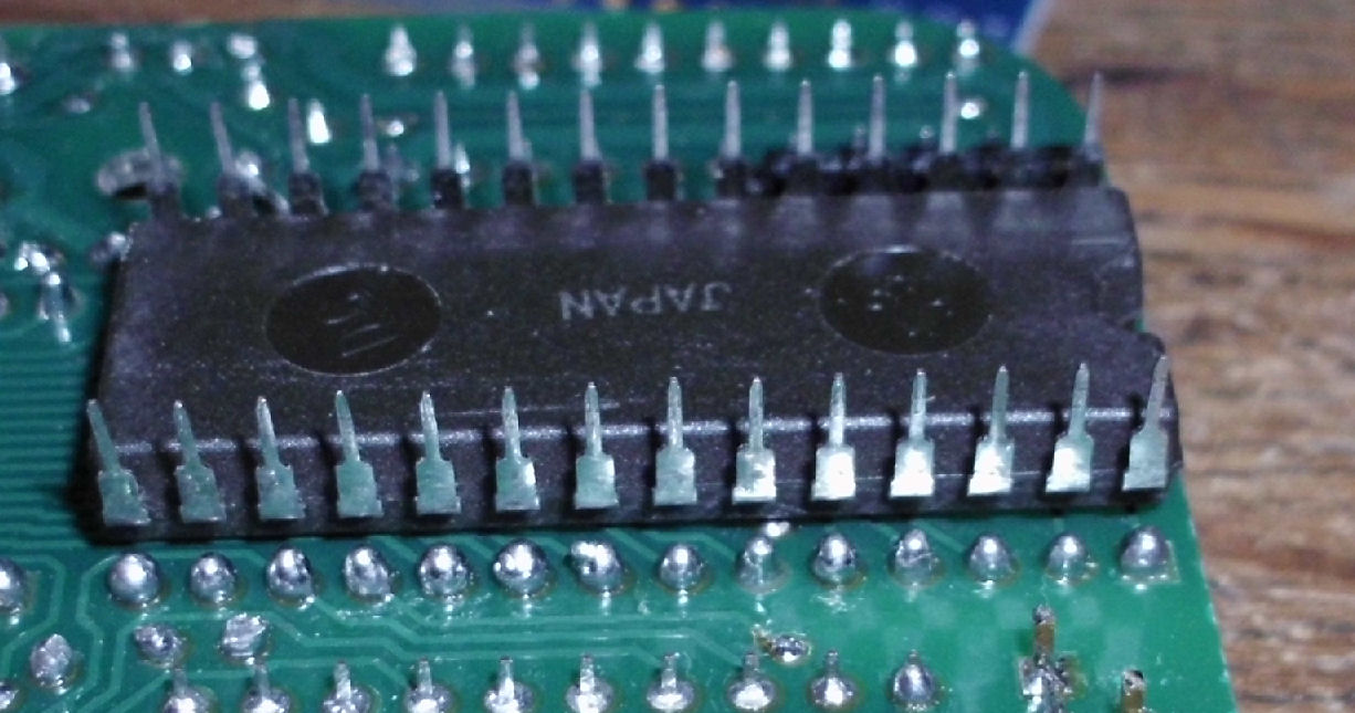
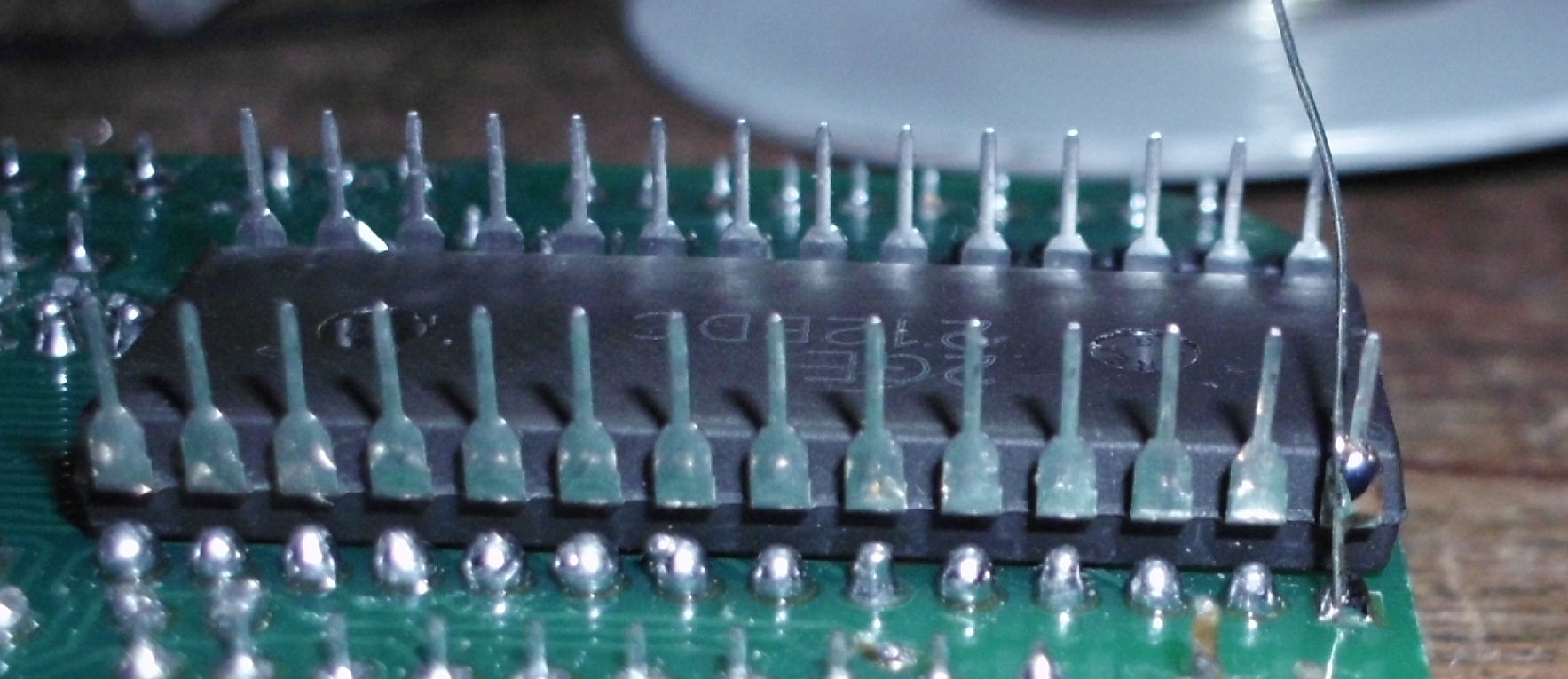
![[kit]](build/dip_solder1.jpg) DIP solder, start w/ one pin
DIP solder, start w/ one pin
DIP solder complete, top
DIP solder complete, bottom
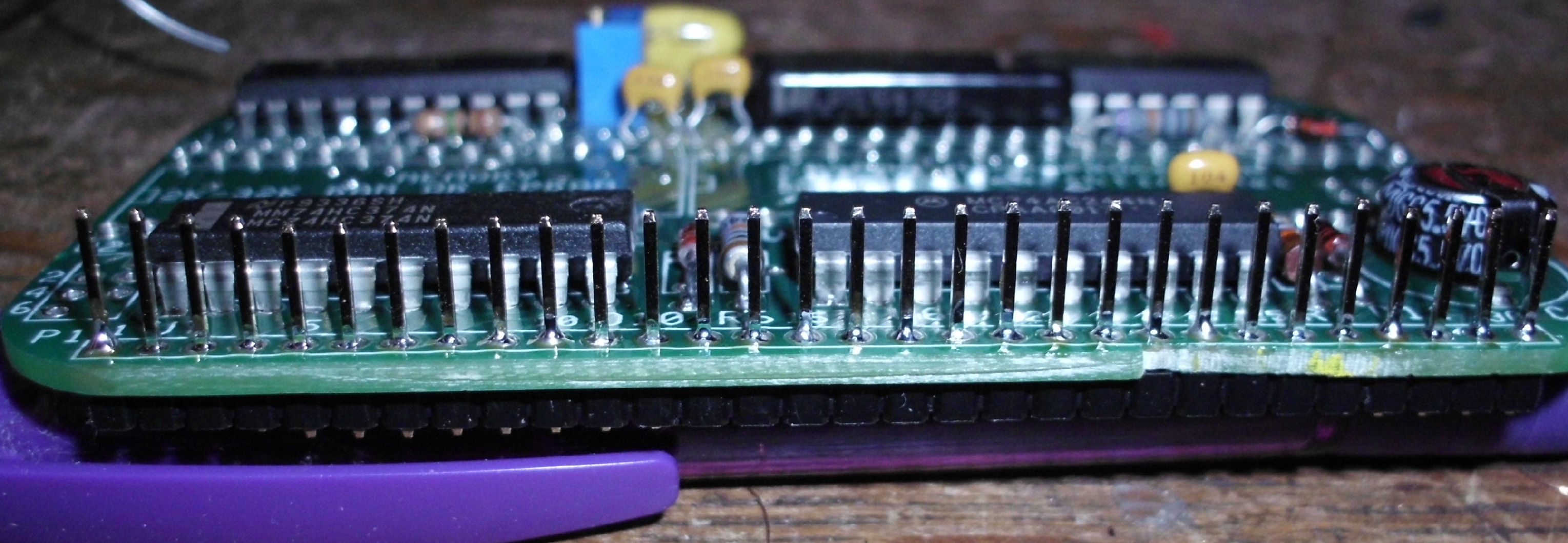
![[kit]](build/header30_done.jpg) 30-pin header, insert from bottom
30-pin header, insert from bottom
30-pin header, from bottom, pins pushed "down"
30-pin header, solder from top
30-pin header, from bottom, open solder joints
30-pin header, use Molex connector to secure pins, resolder from bottom
30-pin header soldered in, from bottom
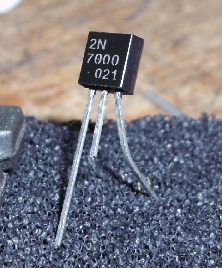
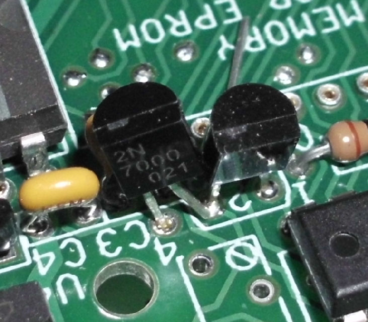
![[kit]](build/fet.jpg) installed FET pins 1, 2, 3
installed FET pins 1, 2, 3
CPU board less RAM & 1802, top
CPU board less RAM & 1802, bottom
![[kit]](build/ram_insrt.jpg) insert RAM carefully
insert RAM carefully
CPU board, completed
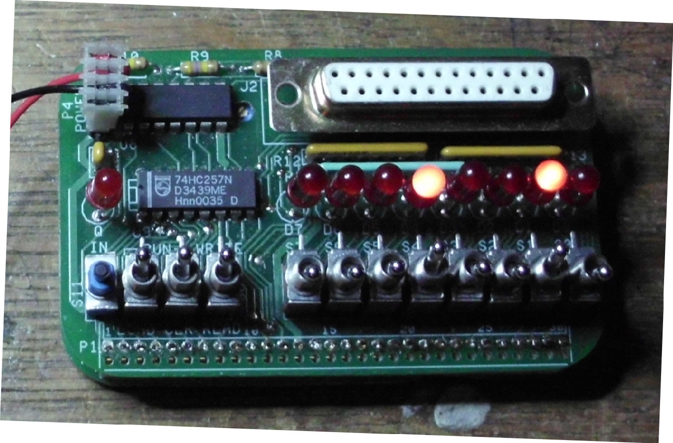
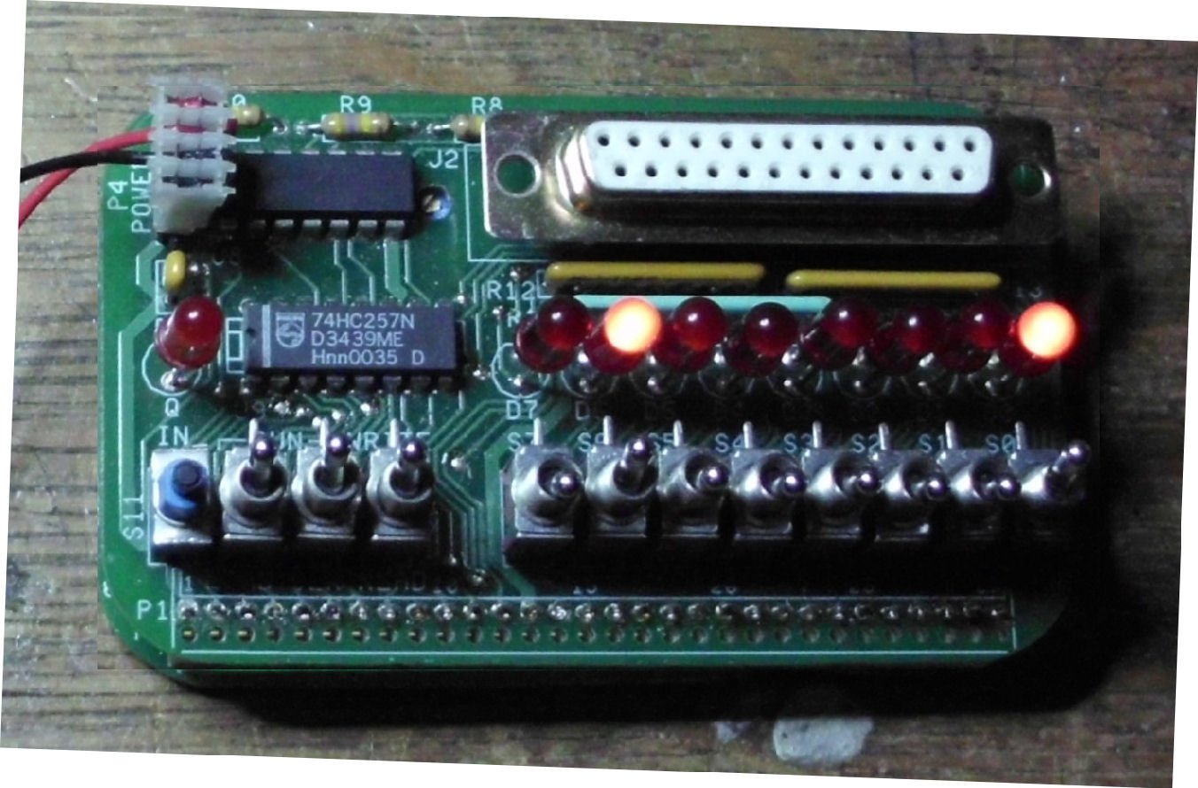
![[kit]](build/cpu_toggle1.jpg) 1802 M/S card, powered up
1802 M/S card, powered up
1802 M/S card, read toggles 1
1802 M/S card, read toggles 2
1802 M/S card, read toggles 3
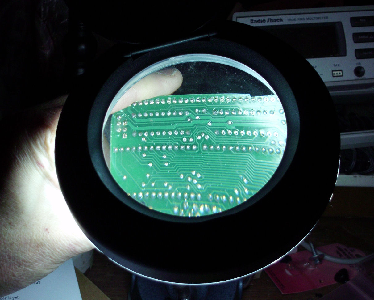
A large magnifier is very useful
plastic insulator under front-panel card. nut provides spacer between boards.
DC power plug, note doubled power and ground pins
compare RAM sockets: low profile socket versus pins-in-board
RAM-only Rev F CPU board, retained short 16-byte programs overnight (12 hours) on supercap backup. Voltage at that time was down to 1.75 volts. Original voltage was near 4.5 volts from three alkaline AA batteries. Temp was low 60's.
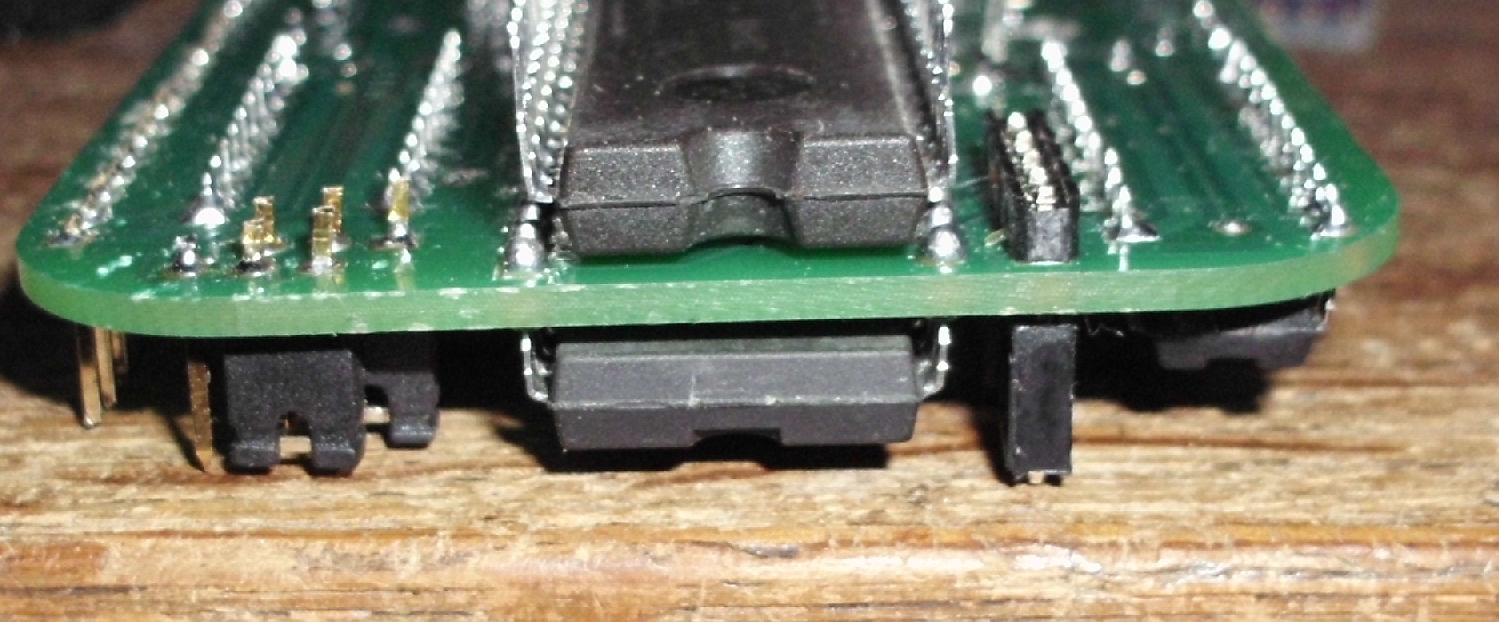
Revision F only had one ROM or RAM socket. To operate both, they had to be "stacked". To save height above the board, I soldered the RAM under the board, upside down. This was not entirely successful in the long run, but I got it to work. - Herb, 2016.
![[kit]](build/stack_hdw.jpg)
Possible hardware to mount stacked RAM/ROM
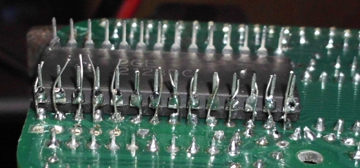
![[ram under]](build/ram_under_board_6.jpg)
loose RAM chip under CPU board RAM/ROM, w/ pins in PC board.
end view of loose RAM under CPU board
Tinned copper uninsultated wire, because socket pins too short to "touch" RAM IC pins.
RAM upside down under board, solder 4 corners first.
RAM upside down under board, solder one side.
RAM upside down under board. one side soldered
RAM upside down under board. one side soldered and trimmed
RAM upside down under board. Socket pins popped up
when pin overheated. With care I reheated and pushed down.
RAM upside down under board. All pins soldered and trimmed.
It was a challenge to solder up. The socket pins got hot and popped up, but I fixed that by touching up. This method would have been easier if I had used a low-profile socket instead of socket pins, as the socket pins would have extended far enough below the PC board, to contact the upside down RAM - no wire needed (look at the photos). and the socket would have held the pins in place too. Oh well...
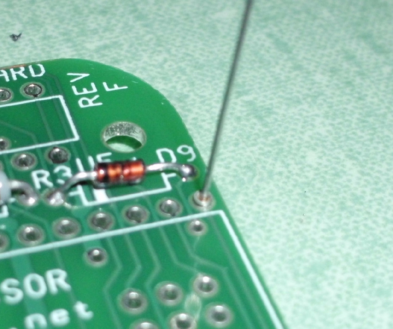
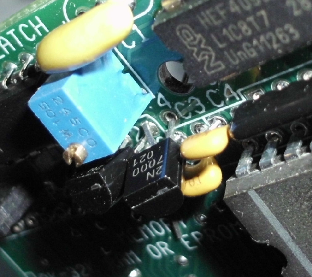
I needed another FET to provide an inverted A15 signal to the ROM - the first FET was in use by the RAM under the CPU board.
![[FET 2]](build/add_fet_7.jpg)
Not much space to add 2nd FET on holes 3 and 4.
Trim gate (center lead) to attach to hole 3, poke drain through hole 4, source lead bent back to go to ROM
I can poke the FET in but can't solder at hole 3, must remove pot to access
desolder braid to suck solder from three potentiometer pins
heat pins and "walk" pot out of holes, successfully. Use braid again to clear solder from holes.
Now solder 2nd FET lead to hole 3 with first FET
Now solder pot back in. Here's the result.
![[serial]](build/pullup_3.jpg)
solder 10K resistor to pin 3 of P2 header for +5Vnote black insulation, cut from hookup wire
add insulation to FET drain pin also trim wire end from pin 3
decided to stack ROM on socket, easier to insert/remove from CPU note pin 20 bent out, that's chip-select for FET/pullup
Soldered resistor to 2nd FET drain wire. ROM and its socket in place. Pullup and FET soldered to pin 20 of ROM
front panel mounted on CPU, crooked but works OK! toggled in "blink Q" program into RAM and it ran.
![[extend]](build/rom_strap4.jpg)
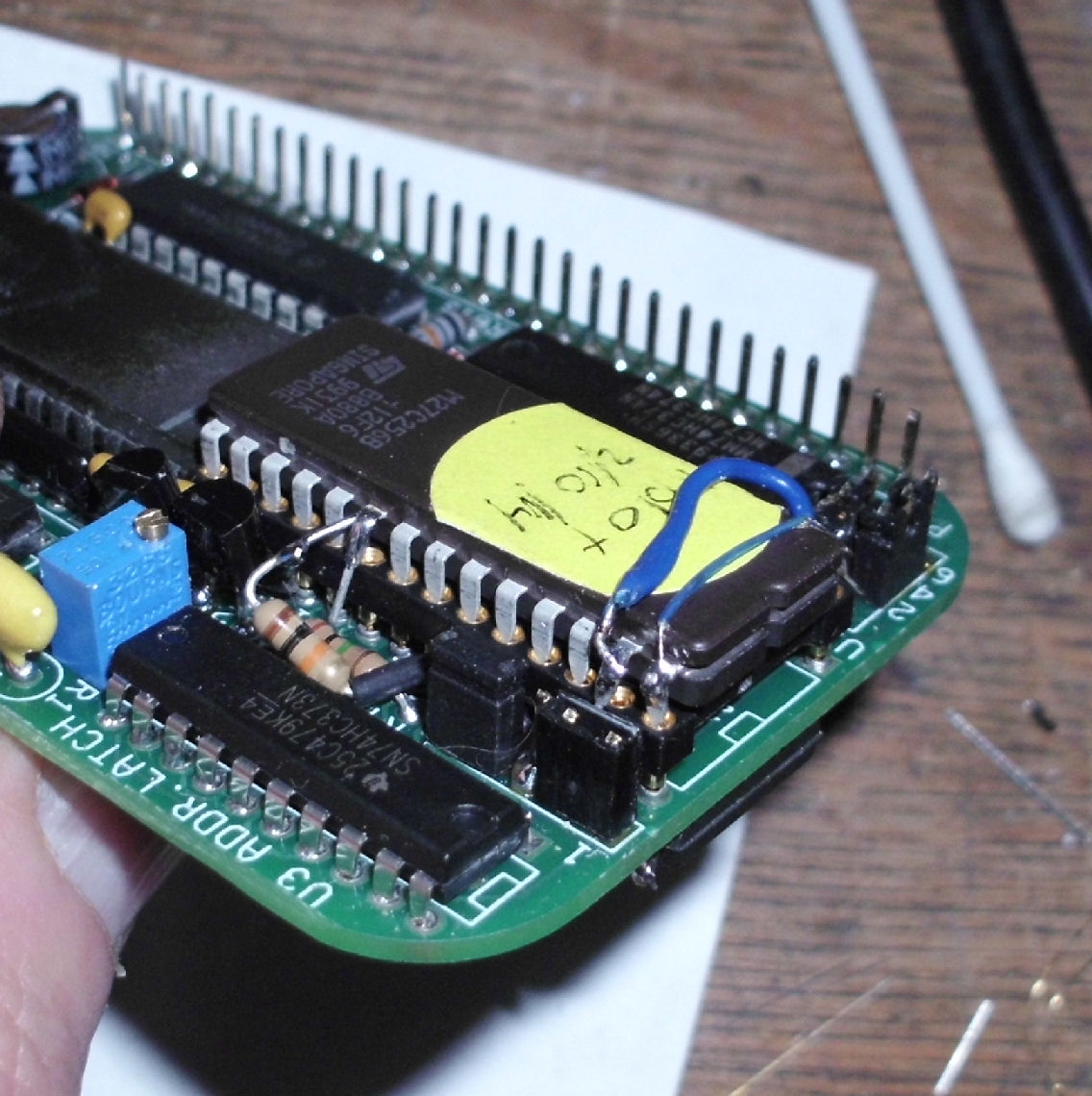
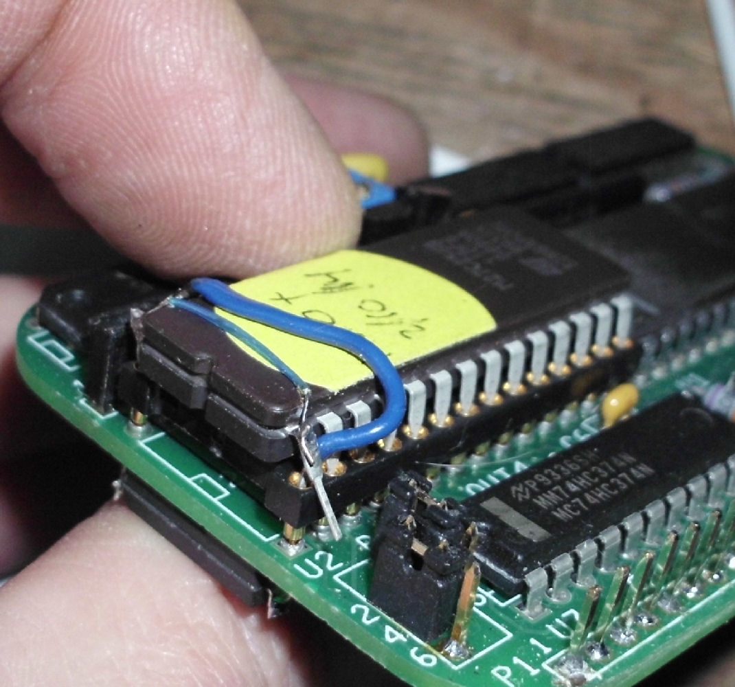
After working on the IDIOT monitor, I found I didn't set up A14 and select on ROM to match connections to RAM in the lower 32K.
Solution: pull ROM pin 1 from socket pin 1, wire ROM pin 1 to pin 28 to pull high;
pull pin from socket on pin 27, wired to inserted in socket pin 1;
and ROM pin 20 pulled from socket and wired to FET to select ROM
ROM strap view end on view, see ROM pins not in socket pins
ROM strap view see wires to 20, 27, 28 on ROM
ROM strap view see wire on ROM pin 1 and socket pin 1
ROM strap view view from above
April 2: pulled ROM from DIP socket and with GREAT effort installed into board-insert pins.
Socket pins inserted into board, have narrow opening, hard to align ROM. Also resoldering moved them around vertically.
lower profile on CPU board with ROM socket eliminated.
Had possible problems with RAM soldered underneath, possible intermittant connections? These are difficult to solder and to visually verify.
Problems cleared up when I found resonator was loose! Soldered resonator and card was back in operation.
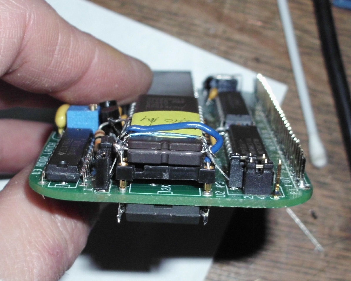
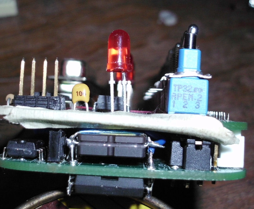
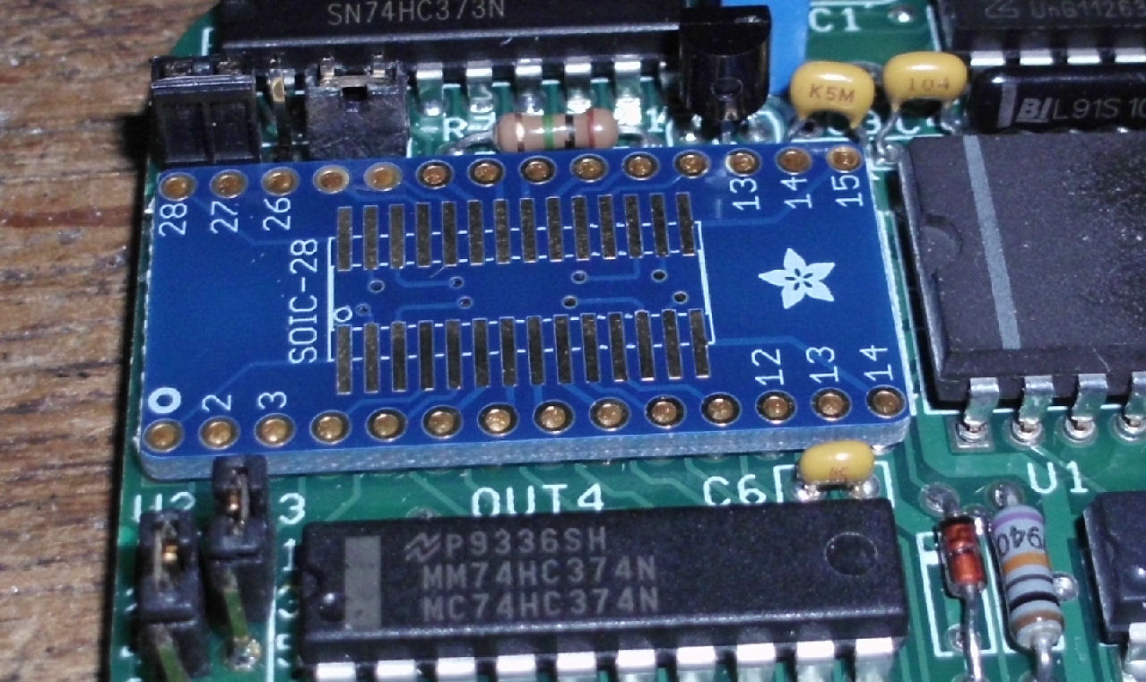
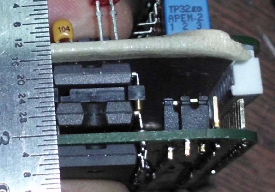
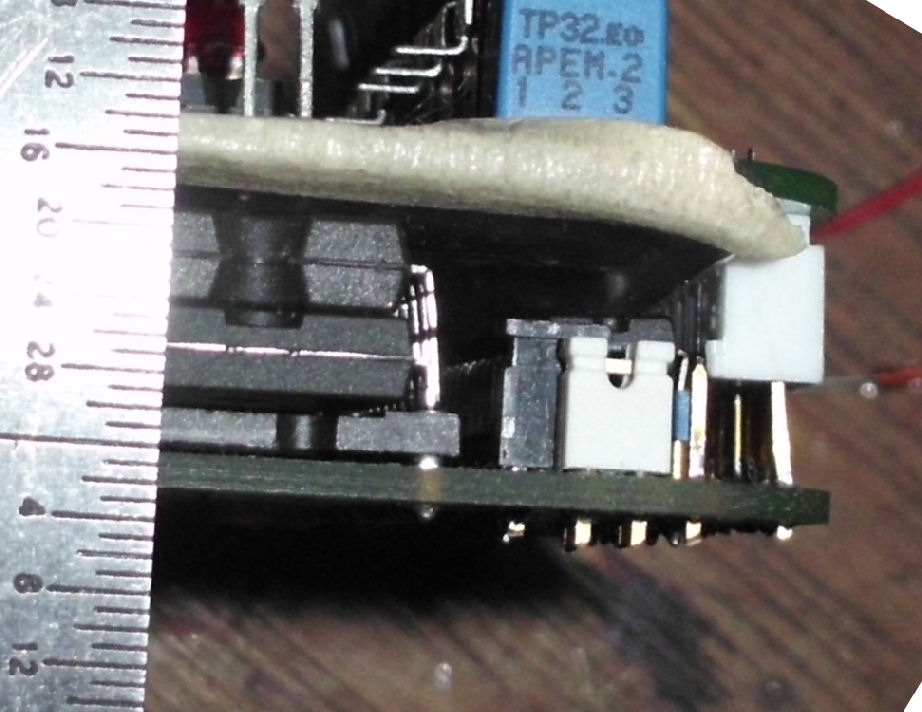
RAM above CPU board on a carrier
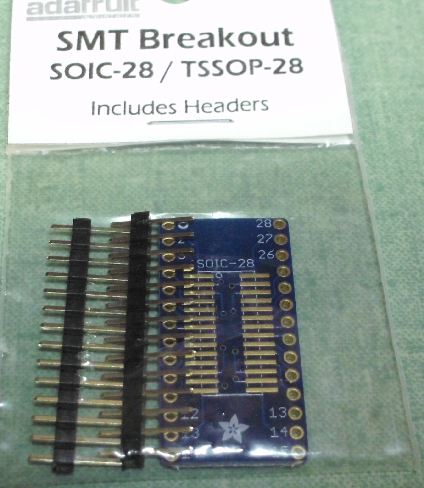
Here's a surface-mount to DIP adapter
SOIC to DIP PC board, loose on top of CPU
Note height above CPU board and a need for a longer 30-pin male header.
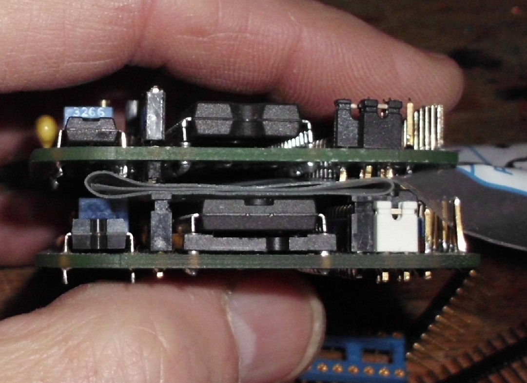
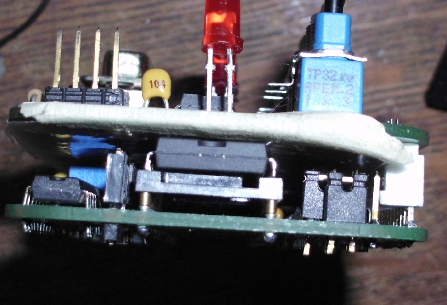
pinned CPU board, socket, RAM stack
pinned CPU board, with RAM, socket, with ROM stacked. HEight .5 inch. RAM also underneath
If you look at the above stack as "RAM below board, pinned board, ROM in pins", the clearance above the CPU board is .25 inch, below is about .25 inch.
socketed CPU board, with RAM, socket, with ROM stacked. Height 1/2 inch.
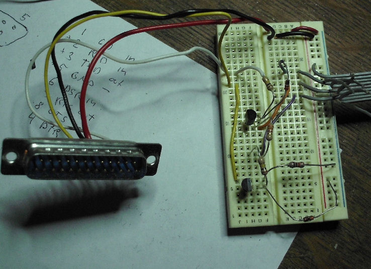
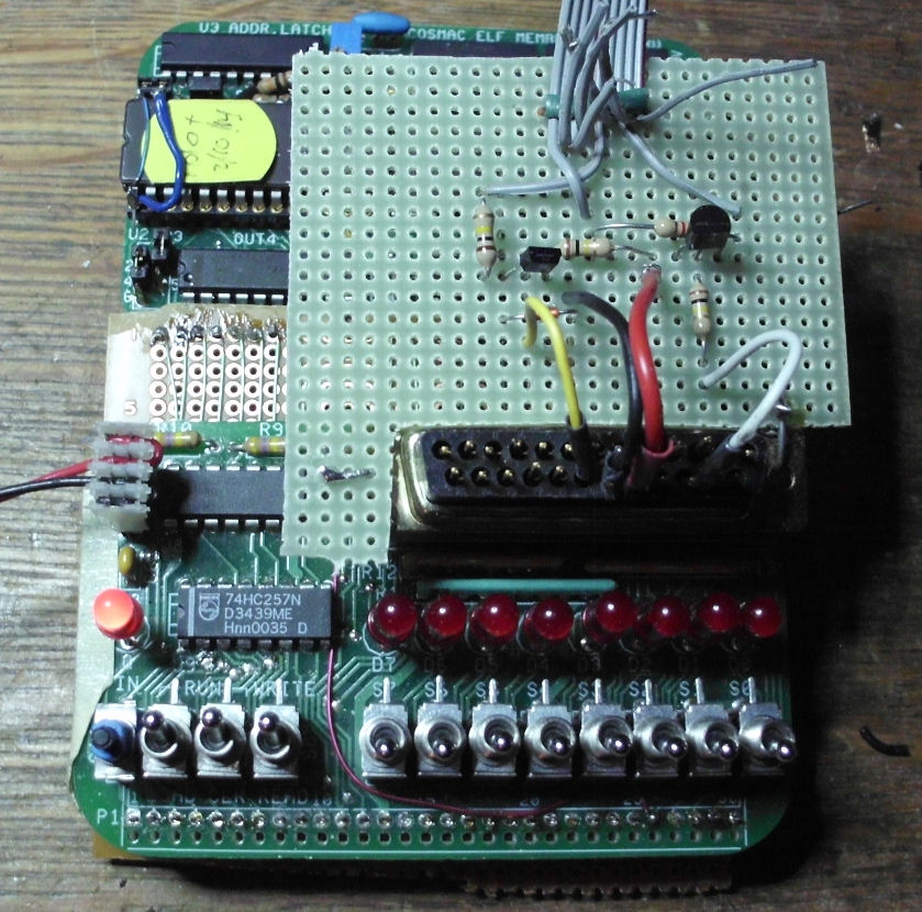
The Revision F only had TTL for serial in and out. I added an external circuit to support "RS-232" voltage levels.
![[serial]](build/serial_bboard.jpg)
![[serial]](build/serial_bboard2.jpg)
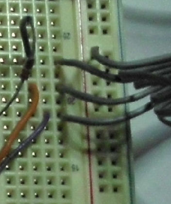
physical layout of serial interface on breadboard. Note colors of wires.
schematic of serial interface.colors on image match wires on breadboard.
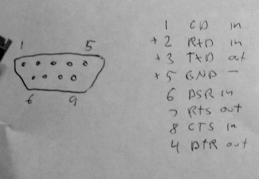
DB-9 male on typical old PC
wire DB-9 femail to breadboard
![[serial]](build/serial_bboard6.jpg)
![[serial]](build/serial_bboard5.jpg)
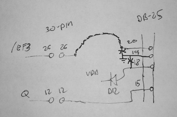
add DB-25 to breadboard
DB-25 pinouts on schematic
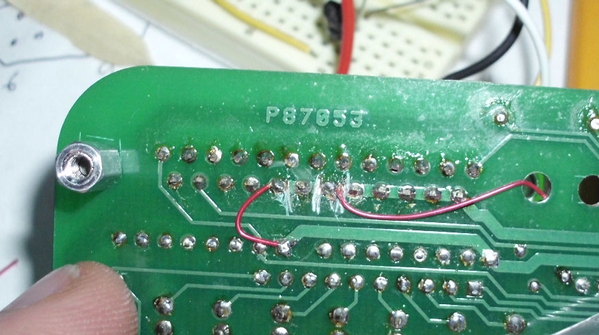
changes to Rev A and later front panel cut DB-25 pins from ground, wire in
cut grounds around pins 18 and 20
DB-25 wired to breadboard and plugged into front panel
note purple/red wire to pin 26 of 30-pin header, that's EF3.
![[serial]](build/serial_bboard8.jpg)
![[serial]](build/serial_bboard7.jpg)
Test of interface under power, showed 3.3K resistor between DB-9 input and output allowed
serial signal to loop back. Solution: disconnect 3.3K resistor from serial input, connect to ground.
Also: I had confused RS-232 TXD and RXD. Solution: swap connections from DB-9 pins 2 and 3.
Also; Q1 emitter was not grounded. Solution: add ground.
Also: diode D2 to DTR or RTS was not necessary, as I connected Q2 to Vcc (5V). Solution: removed D2.
![[serial]](build/serial_signals_1.jpg)
Tests of resulting circuit, no program running:
showed Q1 inverted incoming RS-232 signal to EF3
Showed Q2 inverted outgoing Q signal to RS-232
Proof of interface: jumper at breadboard from EF3 to Q (with line to Q removed)
allowed terminal program to recieve "echo" of transmitted chars.
Also: "toggle Q" program produced inverted output through interface.
April 2: Rebuilt serial interface on perfboard.
April 16: Swapped 2.0MHz resonator to 1.8Mhz. interface operated at 300 baud OK, 1200 baud garbled.
Installed 2.0MHz resonator. With settings of 7 bits, MARK parity, 1 stop, success at 110, 300, 1200 baud.
![[rebuild serial]](build/ser_minus_bd.jpg)
![[rebuild serial]](build/ser_minus_sch.jpg)
April 21: rebuilt interface to make negative supply for interface TXD
.
schematic of Lee Hart updated circuit add diode and cap, to capture terminal TXD negative voltage for interface TXD supply
resulting perfboard circuit
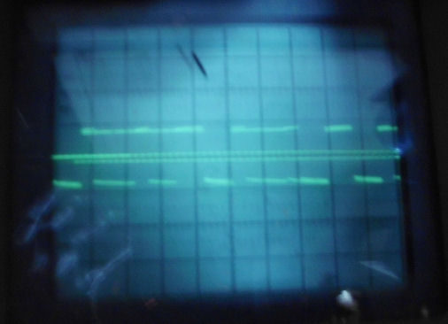
oscilloscope waveform of interface TXD, +/-4.5V
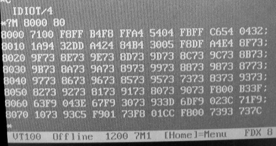
operation of IDIOT at 1200 baud 7 bit mark parity 1 stop (7M1)
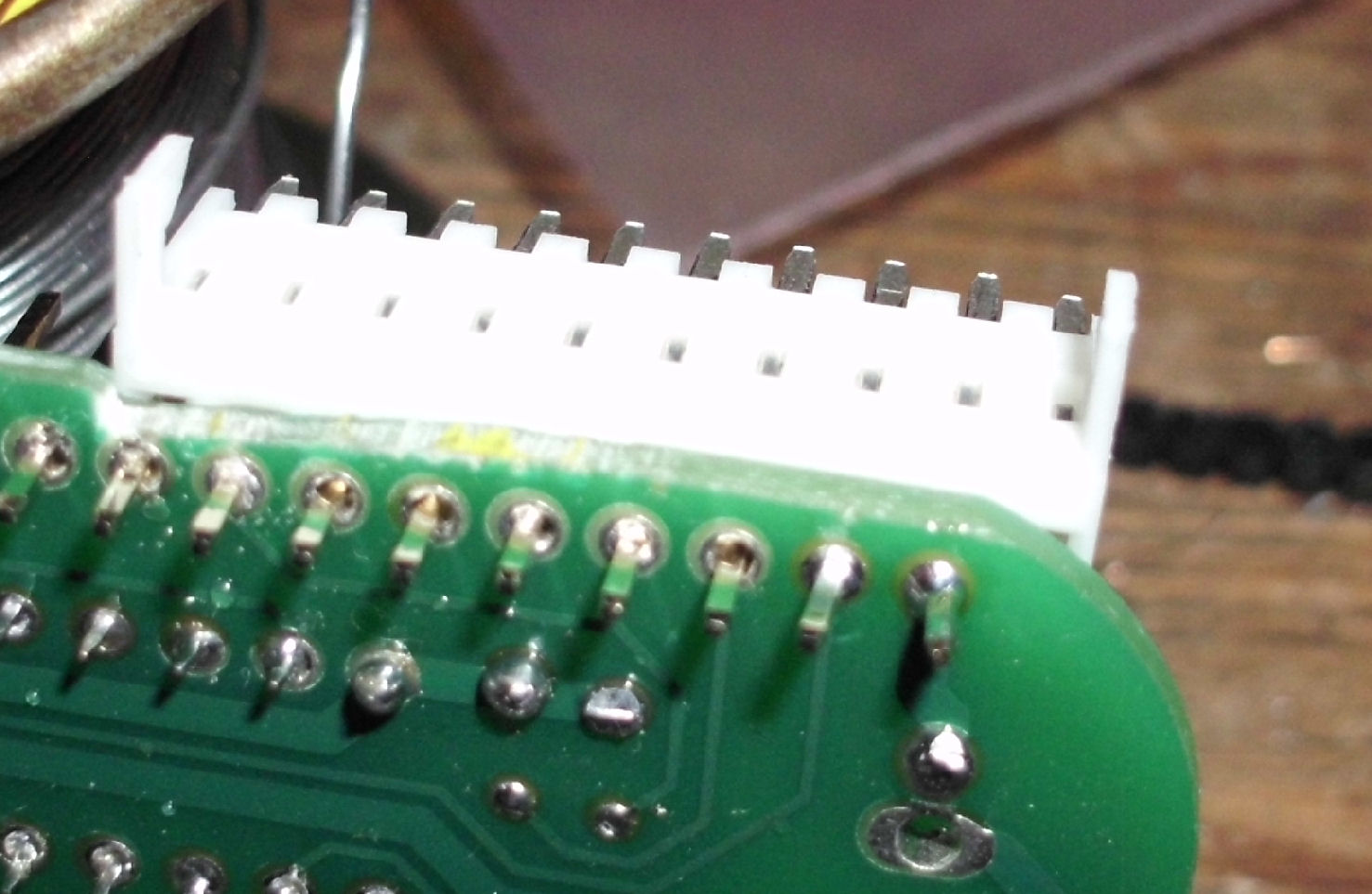
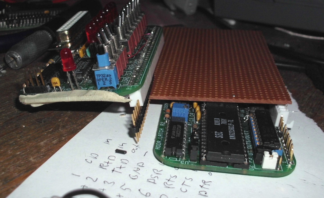
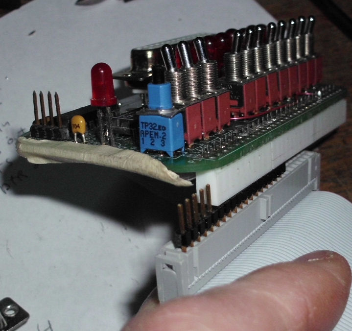
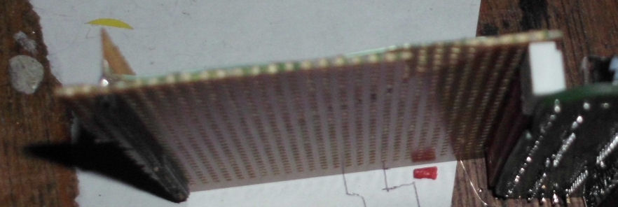
![[extend]](build/extend_pc1.jpg)
Extend with PC board with male header at one end, female header underneath at other
Extend with PC board under front panel, exposes CPU board.
Extend with PC board above CPU board, exposes front panel.
Physically stable but will need supports, feet at various points. Connectors and board have costs.
![[extend]](build/extend_cable1.jpg)
Extend with flat cable with female IDC connectors at either end
Extend with cable wrapped under CPU board, can flip board to examine both sides.
Connect cable via loose header to front-panel, both sides accessable.
Simple construction but might be hard to physically manage, cable will uncurl and flip boards around.
If the cable solution is done this way, replicating the PC board solution, folded cable is avoided:
                                    front panel
                          ==============================
                                                     |||
                                                      |  <---header
                                    cable            | |
                          -----------------------------
                         | |
  CPU board               |
===========================
A female-female IDC cable, with a header jammed into one end to interface to the Molex female of the front panel
Offhand I think the PC-board extender is a physically better solution, and can be hand wired with current stock of M/S card parts. The IDC solution may be worth considering.
![[extend]](build/extender_1.jpg)
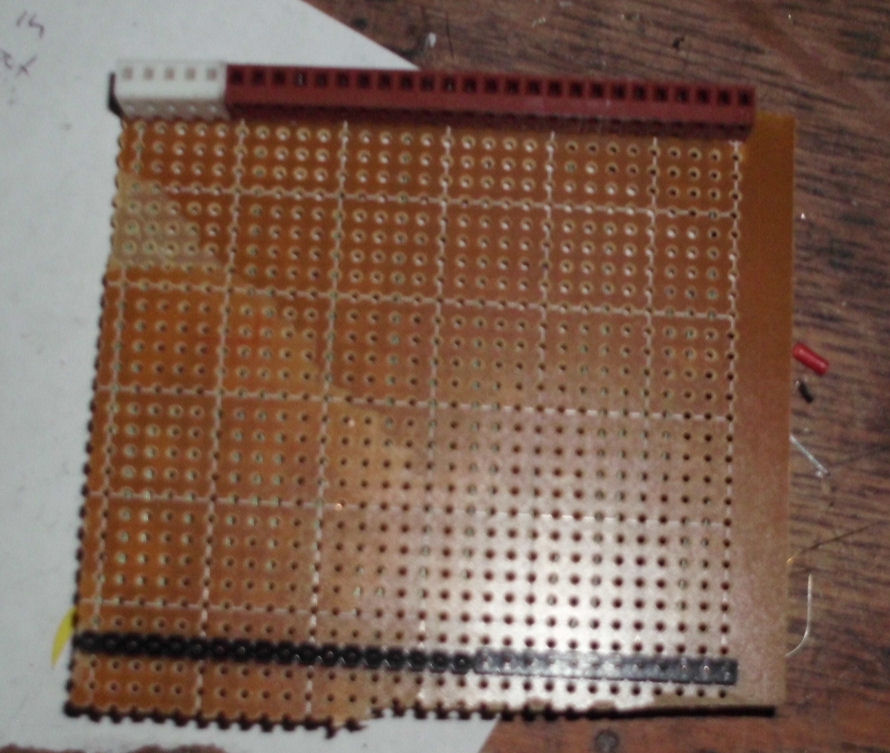
simply wired a header to a Molex connector. Radio Shack board very fragile but provided copper to solder to.
extender view 1
extender 2
extender 3
extender 4
This page and edited content is copyright Herb Johnson (c) 2016. Contact Herb at www.retrotechnology.com, an email address is available on that page..
![[rebuild serial]](build/rom_nosock1.jpg)