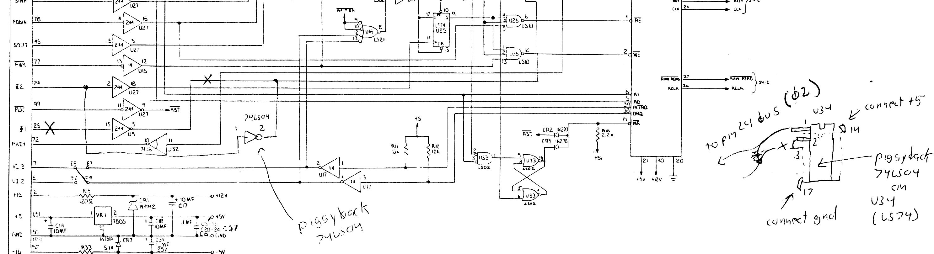
The Versafloppy II card requires an Altair bus clock signal "phase 1" at S-100 pin 24. If your CPU board does not produce that signal, add a 74LS04 chip to the board and invert "phase 2" from S-100 bus pin 25. This is shown on this portion of the board schematic.
I simply solder a 74LS04 (Hex inverter IC) on a convenient chip (U34, a 74LS74) for power and ground (pins 7 and 14) and wire tie a convenient inverter to the appropriate lines. Specifically: place the 04 chip on top of the 74LS74; only solder pins 7 and 14 from the 04 to the 74; bend the other '04 pins OUT OF CONTACT. Unused pins could be cut, this modification uses pins 1 and 2.
With wire (such as wire wrap) tie and solder to pin 1 (inverter input) of the '04 to S-100 pin 24. Do likewise with pin 2 (inverter input) to the flip flop input which normally recieves phase two (see the schematic). In addition you will have to remove from the circuit the bus buffer for the phase 2 line. (the 74LS244 buffer, see schematic). - Herb Johnson